Out With Organic, In With Glass? DNP Unveils Glass Core Substrate Tech For Chips

As the chip industry develops more sophisticated processors with higher heat dissipation requirements, some companies are moving to chiplet-based designs. is becoming more and more important. Large and highly complex chips such as Nvidia’s H100 and advanced multi-chip solutions such as Intel’s Data Center Max GPU (Ponte Vecchio) bring new requirements to packaging materials. To that end, Dai Nippon Printing (DNP) is showcasing a new development in semiconductor packaging, the Glass Core Substrate (GCS). The company says it can address many of these challenges.
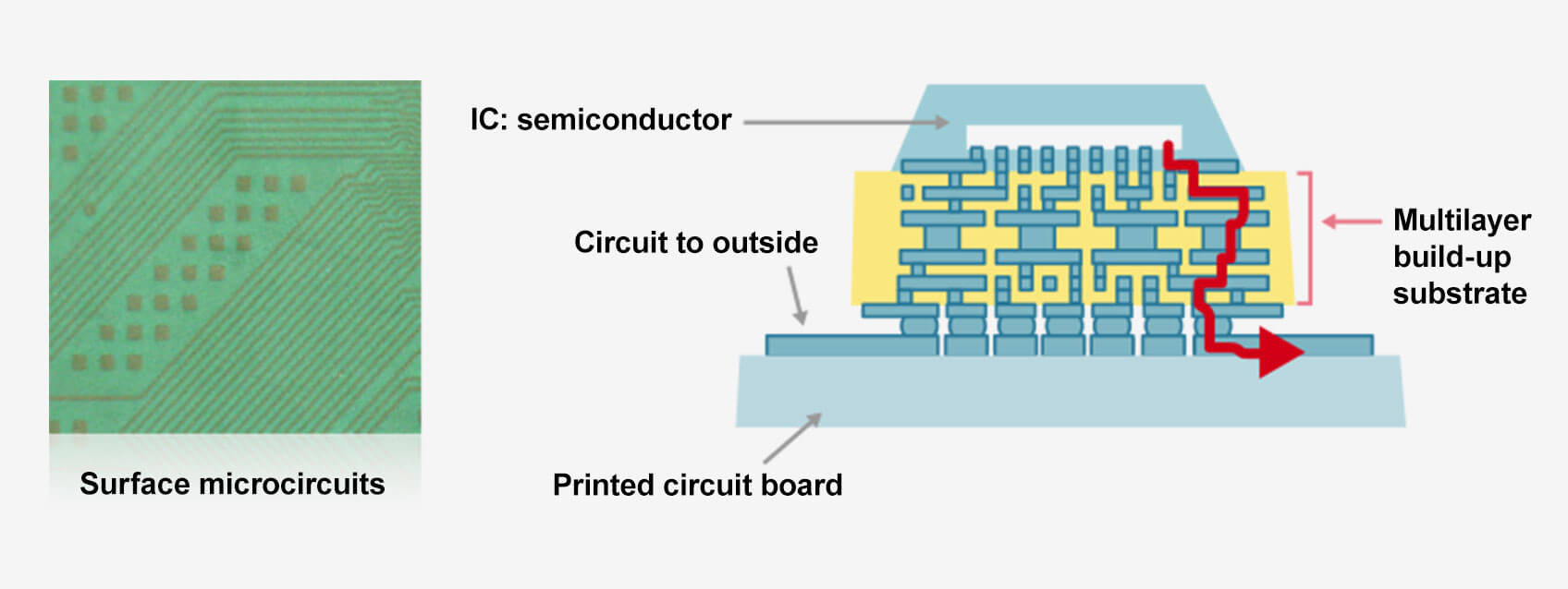
Modern chips are typically mounted on a Fine Pitch Substrate (FPS) and then placed on a Multi-Layer High Density Interconnect (HDI) substrate.Latest state-of-the-art CPU/GPU HDI boards Ajinomoto Build-up FilmAccording to the manufacturer, it combines an organic epoxy resin, a hardener and an inorganic particulate filler (ABF). It is easy to use, allows for high-density pitching (allows for high-density metal wiring), has sufficient insulation properties for modern chips, high rigidity, high durability, low thermal expansion, etc.
Are ABF and other organic resin-based substrates good enough for chiplets? This is quite a challenge as it requires high density metal writes. This increased power requirement puts additional pressure on the outside infrastructure of the circuit. Finding new materials for use within the core composition of chips within the semiconductor industry has been an intense pursuit for many years.
One such company in the semiconductor industry is Dai Nippon Printing (DNP), which claims that its HDI substrates with glass cores have superior properties compared to organic resin-based substrates. I’m here. According to Dainippon, the use of glass-core substrates (GCS) allows for finer pitch and therefore very high-density wiring because it is stiffer and expands less at high temperatures. The schematic provided by DNP omits the fine-pitch substrate entirely from the packaging, suggesting that this part may no longer be needed.

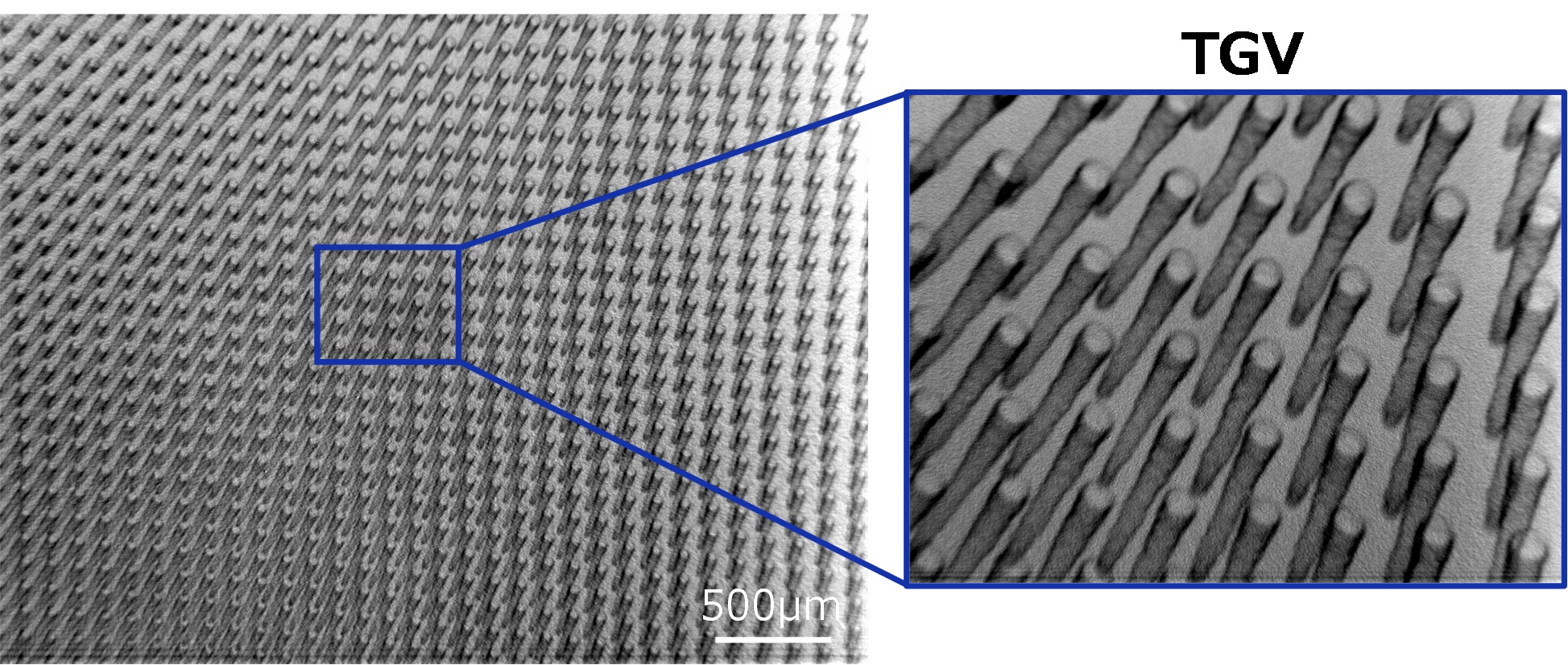
Perhaps most notably, DNP claims that its glass core substrates can offer high through glass via (TGV) densities with high aspect ratios (compatible with FPS). The aspect ratio in this case is the ratio of the glass thickness to the via diameter. As the number of vias increases and the ratio increases, the board becomes more difficult to handle and more difficult to maintain stiffness.
Glass is considered to be more rigid than organic resin-based substrates, which offers some advantages, but adhesion between glass and copper (or other metal wires) remains a major adhesion challenge. The glass substrate developed by DNP ensures adhesion with an aspect ratio of 9 and enables fine-pitch wiring. The company says that because GCS has only a few thickness constraints, it has a lot of latitude when it comes to maintaining a balance between thickness, warpage, stiffness and smoothness.
Dai Nippon Printing manufactures out-coupling reinforcement structures for LCDs and scattering for backlight modules, so it has extensive experience in mass production of glass-based structures. On the other hand, DNP is not the only forward-looking hard glass application specialist in manufacturing HDI substrates for advanced chips or multi-chiplet solutions.Corning have been searching The field hasn’t seen the technology used commercially in mass-produced chips or multi-chip modules for some time.
sauce: Dai Nippon Printing


