Samsung’s $15 Billion R&D Complex to Overcome Limits of Semiconductor Scaling

Samsung broke ground on Friday on a new semiconductor research and development complex that will design new manufacturing processes for memory and logic and conduct fundamental research on next-generation technologies and materials. The company plans to invest his 20 trillion KRW ($15 billion) in new R&D facilities by 2028.
To create more competitive logic and memory chips, companies like Samsung are using new materials (fins, gates, contacts, dielectrics, etc.), transistor architectures, manufacturing techniques, and the design of actual devices. While companies often physically separate basic research from the development of actual process technology, new R&D centers will run nearly everything except device design.
The new facility will not only handle advanced research on next-generation transistors and memory and logic chip manufacturing processes, but will also explore new technologies to “overcome the limits of semiconductor scaling.” Essentially, this means researching new materials and manufacturing techniques, and developing actual production nodes. Considering all these R&D operations have to be massive today, it’s not particularly surprising that Samsung will need to invest his $15 billion in the center over the next six years.
Distributing basic research and applied development work across different locations can help bring in new talent (for example, people with academic backgrounds may be reluctant to relocate far from their current homes). There is a possibility). However, with feedback from different departments, disagreements can arise within a single company. Slower. Ideally, pathfinding and research scientists, developers designing new production nodes, fab engineers, and device developers should collaborate on the site and get feedback from each other. But Samsung’s new R&D hub isn’t meant for this, but it can still bring scientists and node developers together. This is a big problem.
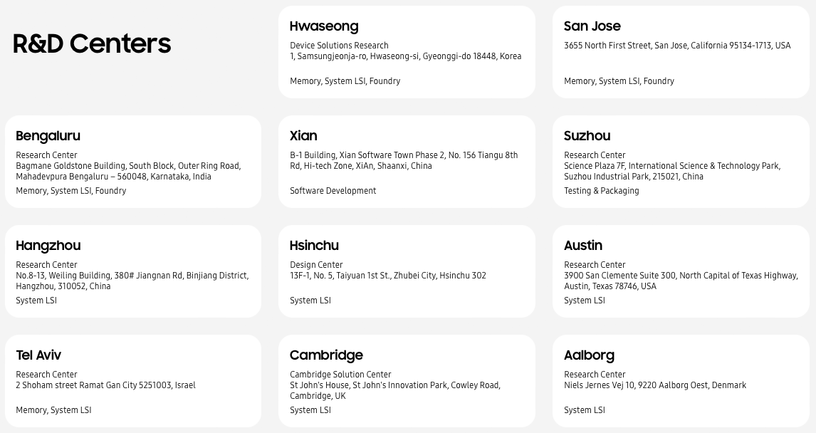
The new R&D center is located on Samsung’s campus near Giheung, South Korea and occupies approximately 109,000 square meters.2 (~20 soccer fields). To put this figure into a more relevant context, Apple’s headquarters, Apple Park, occupies about 259,000 square meters.2 Over 12,000 employees do everything from administration to research to product development.
The new R&D facility will combine Samsung’s existing R&D line in Hwaseong (which handles memory, system LSI, and foundry technology) with Pyeongtaek’s Pyeongtaek, which can produce both DRAM (using 10nm-class technology) and logic chips. It works in conjunction with the company’s production facilities. (Using 5nm-class nodes and below).Samsung’s 12th Semiconductor research and development center. Meanwhile, it will be the company’s first semiconductor research and development facility of this scale.
Three years ago, Samsung announced plans to spend 133 trillion won ($100 billion today, $115 billion in 2019) on semiconductor research and development by 2030. A single R&D facility would fit perfectly with this plan.
Hyung Kyung Kye, who is also head of the Device Solutions (DS) division, said, We hope that this new beginning will lay the foundation for sustainable growth of our semiconductor business. ”
sauce: samsung


