
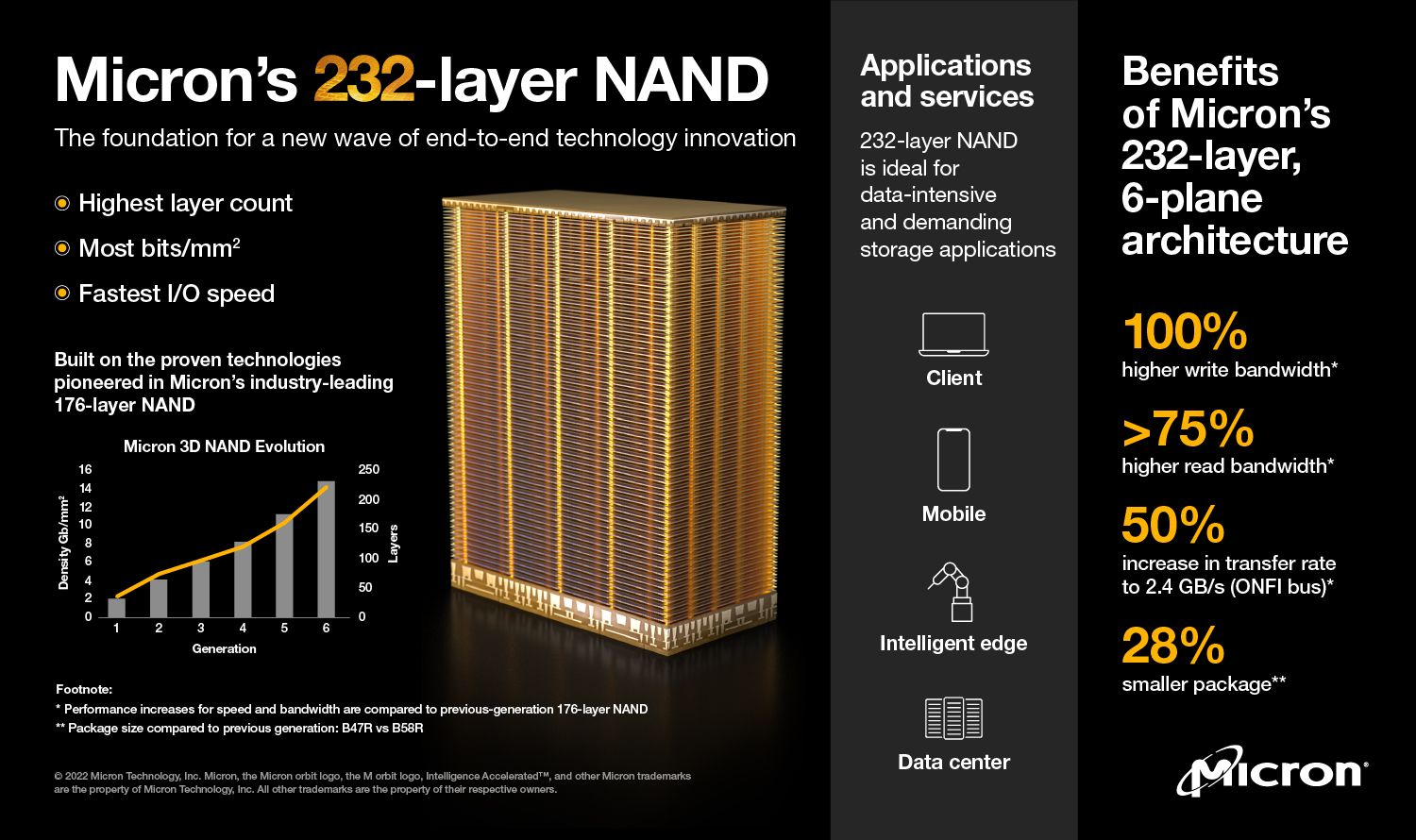
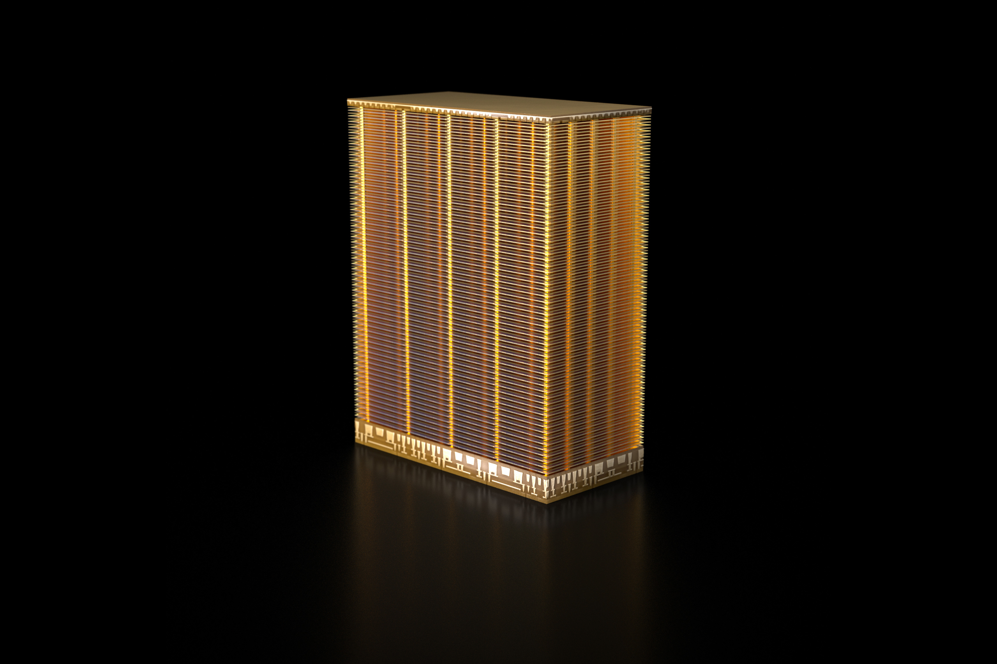
Prior to next week’s Flash Memory Summit, Micron announced this morning that it has begun shipping the next generation of 232-layer NAND. The sixth generation of Micron’s 3D NAND technology, the 232L, will offer both improved bandwidth and increased die size. In particular, we are announcing Micron’s first 1T-bit TLC NAND die, which is currently the densest in the industry. According to the company, the new NAND has already been shipped to customers, and the quantity of Crucial SSD products is limited and will increase further later this year.
At the Investor Day event in May, Micron first unveiled 232L NAND, revealing that NAND will be available this year and that the company plans to increase production by the end of the year. And while that yield is still rising, Micron’s Singapore fab has released enough new NAND to announce that Micron is shipping, despite apparently limited quantities. Can already be produced.
From a technical point of view, Micron’s 232L NAND is further based on the basic design elements that Micron has refined in its generation. That’s why we’re revisiting the String Stack design with Micron, which uses a pair of 116-layer decks from the previous generation’s 88-layer. The 116-layer deck is noteworthy, as this is the first time Micron has been able to create a single deck with more than 100 layers. This is a feat that was previously limited to Samsung. This allows Micron to produce state-of-the-art NAND with just two decks. This may not be possible any longer, as companies are driving designs with a total of more than 300 layers.
Micron’s NAND decks continue to be built on Charge Trap’s CMOS Underarray (CuA) architecture, with most of the NAND logic located underneath NAND memory cells. Micron has long cited this as giving the continuous benefits of NAND density, which is again shown in their 232L NAND. According to the company, it has achieved a density of 14.6 Gbit / mm.2, 176L NAND is about 43% denser. It’s also 35% to 100% more dense than competing TLC products, according to Micron.
| Micron 3D TLC NAND flash memory | ||
| 232L | 176L | |
| layer | 232 | 176 |
| deck | 2 (x116) | 2 (x88) |
| Die capacity | 1 terabit | 512 gigabit |
| Die size (mm2). | ~ 70.1mm2 | ~ 49.8mm2 |
| Density (Gigabit / mm2). | 14.6 | 10.3 |
| I / O speed | 2.4 MT / s (ONFi 5.0) |
1.6 MT / s (ONFI 4.2) |
| Program throughput | ?? | ?? |
| airplane | 6 | Four |
| CuA / PuC | yes | yes |
The increased density has allowed Micron to finally produce the first 1Tbit TLC dies. This means that from a commercial standpoint, Micron can also manufacture 2TB chip packages by stacking 16 232L dies. This is good news for SSD capacity and is often limited by the number of packages that can be deployed at the high end. However, less capacity can reduce performance because less parallelism is reduced when fewer packages are implemented.
At the same time, Micron is also working on the size of the chip package, which means that the larger capacity means that the die size is larger on a generational basis (estimated about 70.1mm).2 Given the Micron density numbers, they are still shrinking the chip package by 28%.As a result, single-chip packages have been reduced from 12mm x 18mm (216mm).2) ~ 11.5mm x 13.5mm (~ 155mm)2). Therefore, for Micron’s downstream customers, the combination of Micron’s NAND high capacity and physically small packages reduces the amount of space device manufacturers allocate to NAND packages, or goes in the opposite direction for more packages. It means that you can try to stuff it. In a similar space.
In addition to increased density, the latest generation of Micron NAND allows the company to upgrade its hardware to take advantage of new I / O technology or implement its own improvements to increase transfer speeds. increase. The big news here is that Micron has increased the number of planes in the NAND die from 4 to 6 to further improve the parallelism available in each die. Quad (4) plane designs have become commonplace in previous generation NANDs, and the higher the NAND density, the more planes the transfer rate will have to accommodate these higher densities. Micron has confirmed that the 232L NAND plane provides independent reads, but it’s not very clear what kind of wordline dependencies remain for writes.
This increased parallelism and increased internal transfer speeds have allowed Micron to significantly improve read and write speeds on a die-by-die basis. According to the company, the read speed has improved by more than 75% compared to the 176L generation NAND, and the write speed has completely doubled in the meantime.
Coupled with this, Micron also implements the latest generation of ONFi in its peripheral logic. Completed in 2021 and currently deployed in the first NAND products, ONFi will increase controller and NAND transfer speeds by 50% to 2400 MT / s. ONFi 5.0 also introduced a new NV-LPDDR4 signaling scheme. It is available at the same 2400 MT / s rate, but consumes less power because it is based on LPDDR technology. According to Micron, energy transfers per bit can be saved by more than 30%, significantly reducing energy consumption. As always in this type of comparison, it is worth noting that the increase in bandwidth outweighs the energy savings (50% vs. 30%). Therefore, the overall energy consumption of high performance products operating in is expected to increase. The fastest speed supported by Micron’s 232L NAND.
In terms of commercialization, Micron is marketing the 232L NAND as a full stack replacement for the 176L NAND. In short, Micron believes it’s suitable for everything from mobile and IoT to client and data center products. To that end, the company has already made its first shipments to customers, including its significant subsidiaries. As with previous generations of Micron NAND, by starting early with Crucial, the company uses the new NAND to develop full-featured products and gain hands-on experience before incorporating them into their enterprise equipment. can do. Interestingly, however, Micron hasn’t announced any new Crucial products at this time. This strongly suggests that Crucial will start implementing new NAND in existing products. In that case, important customers need to pay attention to what’s happening and the revision of the drive they buy. Large 1Tb dies can affect the performance of products originally designed around 512Gbit dies.
In summary, today’s announcement should be the tip of the iceberg for Micron’s 232L shipment. Micron’s plans predict that volume will continue to grow until the end of this year, requiring that the volume of next-generation NAND shipped be significantly higher than these initial volumes. Ultimately, this means that products with 232L NAND will be relatively sparse this year and will recover in 2023 following increased volume. As a result, Micron’s 232L NAND is actually shipping, but from the consumer’s point of view, it still takes months (or more) to see it become a common fixture on SSDs and other products. There is a possibility.


