
Samsung teased With GDDR7 memory development underway in October last year, the company has not disclosed any other technical details of the upcoming specification.However, cadence recently introduced It was the industry’s first verification solution for GDDR7 memory, and in the process revealed quite a few additional details about the technology. After all, GDDR7 memory uses PAM3 and NRZ signaling and supports many other features with the goal of achieving data rates as high as 36 Gbps per pin.
Lessons from a short history of GDDR
Broadly speaking, the evolution of GDDR memory in recent years has been straightforward. New memory iterations have increased signaling rates, increased burst sizes to accommodate those signaling rates, and improved channel utilization. But none of them increased the memory cell’s internal clock substantially. For example, GDDR5X and then GDDR6 increased the burst size to 16 bytes and then switched to dual channel 32 byte access granularity. Each generation of technology is not without its challenges, but ultimately industry players have been able to increase the memory bus frequency with each version of GDDR in order to keep up the performance gains.
But even “simple” frequency increases are becoming less straightforward. This has led the industry to look at solutions other than raising clocks.
With GDDR6X, Micron and NVIDIA have replaced traditional non-return-to-zero (NRZ/PAM2) encoding with four-level pulse amplitude modulation (PAM4) encoding. PAM4 uses four signal levels to increase the effective data transfer rate to 2 data bits per cycle, allowing higher data transfer rates. In fact, GDDR6X is designed to reach the same data rate (or rather signaling rate) as GDDR6, if not faster, due to its burst length of 8 bytes (BL8) when operating in PAM4 mode. I’m here. Higher data rates than GDDR6 can easily achieve.
Four-level pulse amplitude modulation outperforms NRZ in terms of signal loss. PAM4 requires half the baud rate of NRZ signaling for a given data rate, resulting in significantly less signal loss. Higher frequency signals degrade more quickly as they pass through a wire/trace, and memory traces travel relatively long distances in terms of digital logic standards, essentially allowing them to work with lower frequency buses. , which ultimately makes some of the engineering and trace routing easier. Achieve higher data rates.
The trade-off is that PAM4 signaling is generally more sensitive to random induced noise. In exchange for a lower frequency signal, we must be able to correctly identify the double state. In practice, this results in higher bit error rates at certain frequencies. Reducing BER requires implementing equalization at the Rx end and pre-compensation at the Tx end, which increases power consumption. Forward error correction (FEC) is also a practical requirement at higher frequencies (such as PCIe 6.0), although not used in GDDR6X memory.
And, of course, the GDDR6X memory subsystem requires an all-new memory controller and an all-new physical interface (PHY) in both the processor and memory chips. These complex implementations are the main reason why four-level coding has been used almost exclusively in high-end data center networking until very recently, and there is margin to support such state-of-the-art use.
GDDR7: PAM3 encoding up to 36 Gbps/pin
Given the above trade-offs in using either PAM4 signaling or NRZ signaling, it turns out that the JEDEC members behind the GDDR7 memory standard have taken a compromise position instead. GDDR7 memory is set to use PAM3 encoding for high speed transmission instead of using PAM4.
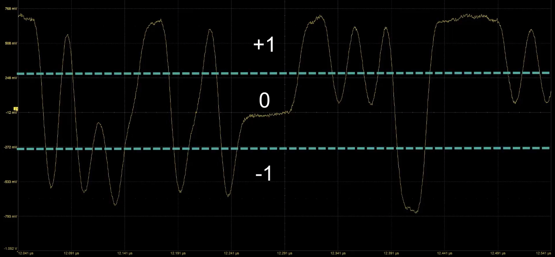
As the name suggests, PAM3 sits between NRZ/PAM2 and PAM4, using 3-level pulse amplitude modulated (-1, 0, +1) signaling to achieve 1.5 bits per cycle (or rather 3 bits or more) can be sent. 2 cycles). PAM3 offers a higher data transfer rate per cycle than NRZ. Reduces the need to migrate to higher memory bus frequencies and the associated signal loss challenges. On the other hand, it requires a looser S/N ratio than PAM4. In general, GDDR7 not only promises higher performance than his GDDR6, but also lower power consumption and implementation costs than GDDR6X.
And for those scoring, this is actually the second major consumer technology introduced using PAM3. He uses PAM3 for USB4 v2 (aka 80Gbps USB) for similar technical reasons. To quote from the first coverage of 2021:
So what exactly is PAM3 doing?
From Teledyne LeCroy on YouTube
PAM3 is a technology that allows data lines to carry either -1, 0, or +1. What the system actually does is combine two of her PAM3 transmissions into a 3-bit data signal. For example, 000 is -1 followed by -1. This gets complicated, so here’s a table.
| PAM3 encoding | ||
| anand tech | Send 1 |
Send 2 |
| 000 | -1 | -1 |
| 001 | -1 | 0 |
| 010 | -1 | 1 |
| 011 | 0 | -1 |
| 100 | 0 | 1 |
| 101 | 1 | -1 |
| 110 | 1 | 0 |
| 111 | 1 | 1 |
| unused | 0 | 0 |
Comparing NRZ with PAM3 and PAM4 shows that the data transfer speed of PAM3 is between NRZ and PAM4. The reason PAM3 is used in this case is that it provides higher bandwidth without the additional restrictions required to enable PAM4.
| NRZ vs. PAM-3 vs. PAM4 | |||
| anand tech | bit | cycle | bits per cycle |
| NRZ | 1 | 1 | 1 |
| PAM-3 | 3 | 2 | 1.5 |
| PAM-4 | 2 | 1 | 2 |
That said, it remains to be seen how much power Samsung’s promised 256-bit memory subsystem with its promised 36 Gbps data transfer speeds will draw. The GDDR7 specification itself has not yet been ratified, and the hardware itself is still being built (this is where tools like Cadence come into play). But keeping in mind that applications for AI, HPC, and graphics are bandwidth-hungry, that bandwidth is always welcome.
Optimizing efficiency and power consumption
In addition to increased throughput, GDDR7 will feature various ways to optimize memory efficiency and power consumption. Notably, GDDR7 supports four different Read Clock (RCK) modes in Bid to enable only when needed.
- Always Running: Always running and stopped during sleep mode.
- Disabled: Stop execution.
- Start with RCK Start Command: The host can issue the RCK Start command to start the RCK before reading any data, and stop it with the RCK Stop command if necessary.
- Start with Read: The RCK automatically starts executing when the DRAM receives a command that involves reading data. It can be stopped using the RCK Stop command.
Additionally, the GDDR7 memory subsystem can issue two independent commands in parallel. For example, bank X can be refreshed by issuing a bank-by-bank refresh command on CA.[2:0]Bank Y can be read by issuing a read command on CA.[4:3] at the same time. GDDR7 also supports Linear Feedback Shift Register (LFSR) data training mode to determine proper voltage levels and timing to ensure consistent data transfer. In this mode, the host tracks individual eyes (connections) and applies the appropriate voltages to optimize power consumption.
Finally, GDDR7 can switch between PAM3 and NRZ encoding based on bandwidth needs. High bandwidth scenarios use PAM3, while low bandwidth scenarios can shift the memory and memory controller down to the more energy efficient NRZ.
Cadence Offers First GDDR7 Verification Solution
JEDEC has not officially published the GDDR7 specification, but this latest technical data dump is available when Cadence launches a verification solution for GDDR7 memory devices. Their solution fully supports PAM3 simulations with real representations, supports binary buses, intensity modeling, and real number modeling.
Validation IP also supports different modes of error injection in multiple fields of the transaction during array data transfer and interface training. Additionally, it comes with a waveform debugger solution to visualize transactions in a waveform viewer for faster debugging and verification.
“The first to market Cadence GDDR7 VIP enables early adopters to start using the latest specifications quickly, ensuring standards compliance and achieving the fastest path to IP and SoC verification closure. ‘ said Cadence’s statement.
When will GDDR7 land?
GDDR7 promises a big performance boost without a big increase in power consumption, but perhaps the biggest question from the technical audience is when A new type of memory is set to become available. There is no specific timeframe in which GDDR7 is expected to be released without a firm commitment from JEDEC. But given the work involved and the release of verification systems from Cadence, it’s not unreasonable to expect GDDR7 to hit the scene alongside next-generation GPUs from AMD and NVIDIA. Note that we tend to introduce new GPU architectures on a two-year cycle. This means that GDDR7 will not arrive in devices until late 2024.
Of course, given that so many AI and HPC companies are working on bandwidth-hungry products these days, it’s possible that one or two of them will soon release solutions that rely on GDDR7 memory. I have. But the massive adoption of GDDR7 will almost certainly coincide with an increase in next-generation graphics boards from AMD and NVIDIA.


