
TSMC held a “first tool-in” ceremony at its Arizona factory this week to celebrate its first U.S. factory, as well as announce plans for a major expansion of its production facility. World’s Largest Foundry Invests Tens of Billions in Next Stage of Fab 21 Near Phoenix, Arizona is. trailing edge node)
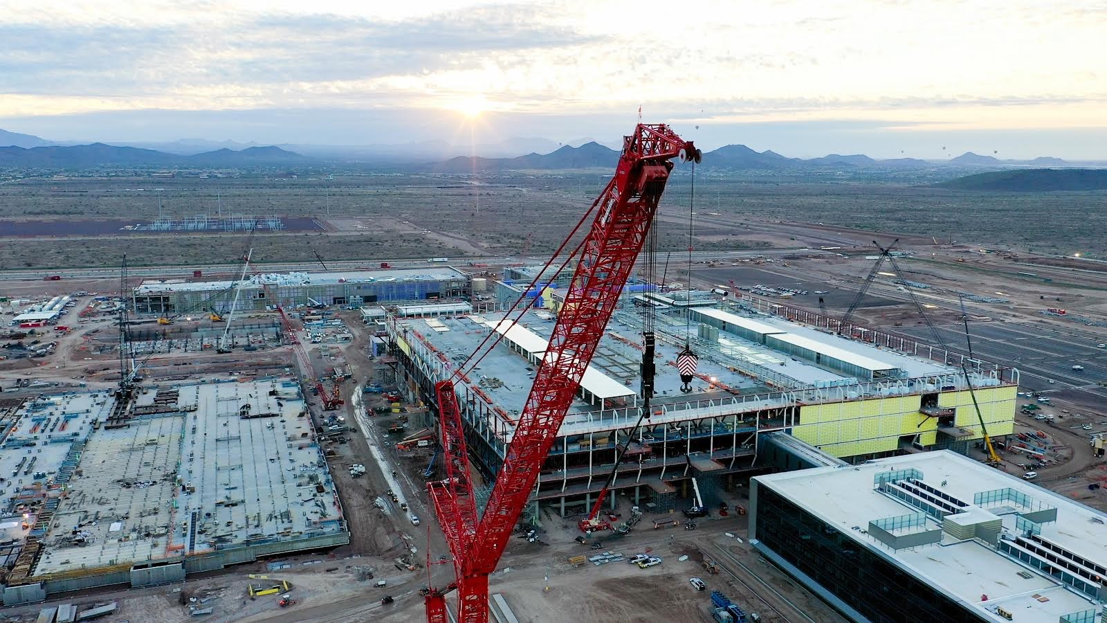
Construction of TSMC’s Fab 21 Phase 1 in Arizona was completed earlier this year, and this week the company began installing production tools at the facility. The fab will be equipped with tools from companies like ASML, Applied Materials, KLA, Lam Research and Tokyo Electroni in the next few quarters and is expected to go live in early 2024. The fab will use a variety of process technologies to manufacture the chips. It belongs to TSMC’s N5 family, which now includes N5, N5P, N4, N4P, and N4X nodes. The exact number depends on the actual technology and design, but the fab’s capacity at this stage is approximately 30,000 wafer starts per month (WSPM).
Companies such as AMD, Apple, and NVIDIA are set to execute orders through Fab 21 Phase 1 to manufacture advanced chips in the US for the first time in years.
But that’s not all TSMC has in store for Fab 21. The company has announced that it intends to further expand its U.S. production capacity, install a new production line, and build his second fab at the site.
The new fab in Arizona will expand TSMC’s capacity at the site to approximately 50,000 WSPM, raising TSMC’s total investment in the site to $40 billion. Notably, this topped his initial $12 billion investment TSMC made in its first fab in Arizona by $28 billion, highlighting that new fab costs continue to rise, but It also shows that TSMC is getting used to making bigger infrastructure investments in the US. TSMC expects $10 billion in annual revenue from its Arizona fab. Reuters report. Meanwhile, TSMC’s clients using fabs will generate about $40 billion in revenue selling products made by US foundries.
The second Arizona fab, which is expected to come online in 2026, will produce chips at TSMC’s N3 family of production nodes, including the N3, N3E, N3P, N3S, and N3X, and will start a generation earlier than the first fab. increase. TSMC plans to deliver its first N3 chips to clients in early 2023. So while the fab still represents cutting edge technology at the start, by the time it comes online it will be technically the most advanced fab. TSMC has previously indicated that it will keep its cutting-edge production in Taiwan, mainly because the actual R&D is done in Taiwan.
In terms of capacity, the new Arizona fab, like its existing siblings, will be another “mega fab” in TSMC parlance. So it’s a mid-range fab producing about 25,000 wafers per month. TSMC hasn’t revealed specific production figures for the new fab alone, but it looks like this fab will be a bit bigger, closer to 30,000 WSPM, as fab 21 is expected to deliver 20,000 WSPM. Still, TSMC’s Arizona fab has a total capacity of 50,000 wafers per month, and he’s still one of TSMC’s smaller operations. So even with a second fab line, TSMC’s US operations represent a relatively small portion of the company’s overall chip fab capacity.
Looking ahead, TSMC has already begun construction on its second Arizona fab, and given its normal fab construction schedule, Shell is expected to be completed by early 2024. After that, it will take another two years or so for TSMC to equip it.
Meanwhile, TSMC plans to start producing chips in Taiwan in the second half of 2025 using the N2 node. Over time, the backside power supply increases. Still, not all products require cutting-edge nodes, so TSMC will have no trouble lining up customers for his N3 US domestic capacity.
AMD CEO and Chairman Lisa Su said: “TSMC’s investment and expansion in Arizona is extremely important and mission-critical to both the semiconductor industry and our broad ecosystem of partners and customers. We are excited and look forward to building our highest performing chips in Arizona.”
sauce: TSMC


