
Continuing to report on AMD’s 2022 Financial Analyst Day, there is a problem with AMD’s upcoming RDNA 3GPU architecture and the Navi3X GPUs built on it. So far, AMD has been pretty quiet about what to expect from RDNA 3, but as RDNA 2 approaches its second birthday and the first RDNA 3 product is due to be launched this year, AMD is about GPUs. Architecture that offers some of the first important details.
First of all, let’s talk about performance. Built on a 5nm process (TSMC, arguably), the Navi 3X family aims to improve performance by over 50% per watt compared to RDNA 2. This is as important an improvement as AMD has migrated from RDNA. (1) Go to RDNA 2. And while such a claim from AMD would have seemed flashy two years ago, RDNA2 has given AMD’s GPU team a significant amount of new credibility.
Thankfully for AMD, unlike the transition from 1 to 2, you don’t have to find a way to come up with a 50% improvement based solely on architecture and DVFS optimizations. The 5nm process means that Navi3X is getting a complete node improvement from the TSMCN7 / N6-based Navi2X GPU family. As a result, AMD is expected to be significantly more efficient on its own.
But that said, these days, single-node jumps alone can’t improve performance per watt by 50% (RIP Dennard Scaling). Therefore, there are several architectural improvements planned for RDNA 3. This includes the next generation of AMD’s on-die Infinity cache, and what AMD calls the optimized graphics pipeline. According to the company, the GPU computing unit (CU) has also been redesigned, but to what extent it is unknown.
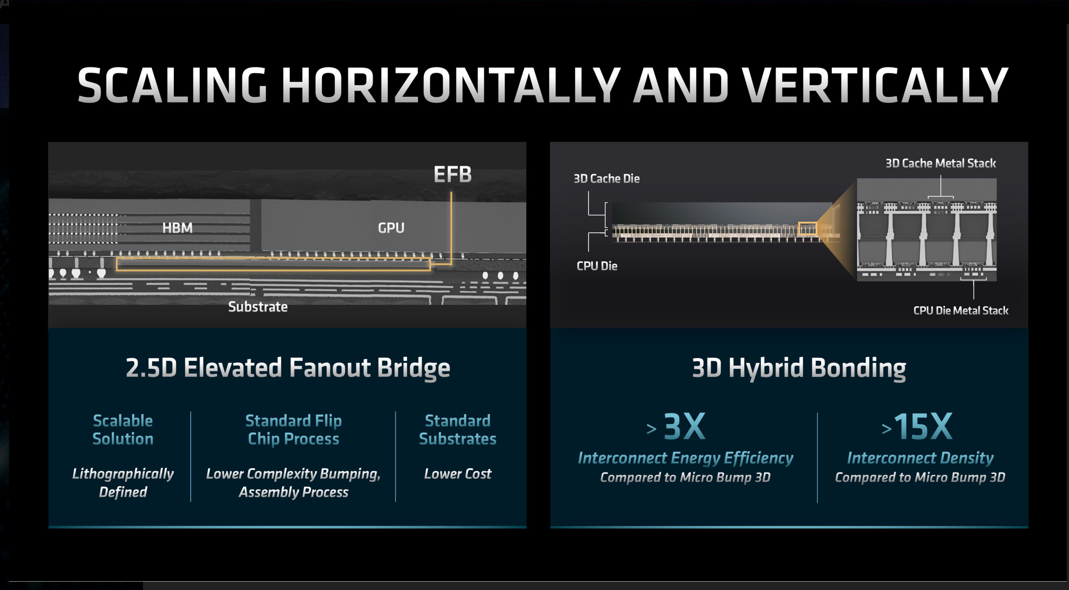
But the biggest news in this regard is AMD’s use of chiplets with RDNA 3 after confirming a year’s worth of rumors and several patent applications. AMD hasn’t said to what extent, but at least one GPU layer (as we know it) is moving from monolithic GPUs to chiplet-style designs with multiple smaller chips. increase.
Chiplets are, in some respects, the Holy Grail of GPU building, as they give GPU designers the option to scale up their GPUs beyond today’s die size (reticle) and yield limits. That said, it’s very difficult to execute the huge amount of data (in the order of terabytes per second) that must be passed across different parts of the GPU, which is very necessary if you need multi. So this is also the Holy Grail. The chip GPU allows you to present itself as a single device. We’ve seen Apple tackle this task by essentially bridging the two M1 SoCs, but this has never been done on high-performance GPUs.
In particular, AMD calls this an “advanced” chiplet design. This monica tends to be thrown when packaging chips using advanced high density interconnects such as EMIB. This is different from a simple design such as the Zen 2/3 chiplet, which simply routes the signal through the organic package. Without enhanced technology. So, waiting for more details on what AMD is doing here, AMD’s form of local Si interconnect (LSI) technology (the MI200 family of accelerators) bridges the two RNDA3 chipsets directly and tightly. To do.
At this time, AMD hasn’t gotten any further into the architecture or Navi3X GPU. Today is a teaser and roadmap update for the analyst market, not an announcement that can only be expected as a Radeon RX 7000 family of graphics cards. Nonetheless, the more formal announcement shouldn’t be too far away, as the first RDNA 3 product will be available later this year. So I look forward to hearing more about the big changes in the nature of GPU design and manufacturing.


