
At next week’s annual VLSI symposium, Intel will present three much-anticipated papers on the progress of its upcoming PowerVia chip manufacturing technology, an implementation of the backside power delivery network the company is developing. Combined with Intel’s RibbonFET technology for gate-all-around transistors, PowerVia and RibbonFET are slated to serve as Intel’s big one-two punch to the rest of the silicon lithography industry, and I believe Intel will store them again2. Introducing two major chip technologies together. Fab leadership position. The combination of the two technologies will be the backbone of Intel’s ‘Angstrom’ era fab node, and with mass production starting next year, Intel’s new technology advancements will be a subject of great importance both internally and externally. And it’s a problem that Intel wants to address.
When it comes to Intel’s chip manufacturing technology, the stakes for Intel’s R&D group couldn’t be higher. Having been the leader of this factory for many years, he has made many mistakes and now has several years to correct course in order not only to regain his lost leadership position, but also to break into the world. are in the midst of efforts to Large-scale consignment of chip manufacturing business.
As a result, VLSI research papers usually do not receive much external attention, but this year was a notable exception. With RibbonFET and PowerVia scheduled to enter mass production next year, Intel is nearing completion of research and development work on the first generation of these technologies. Intel is now at a stage where it can announce to its peers in the VLSI industry the first discoveries in manufacturing complex logic test chips. And to Intel’s investors and other outsiders, Intel can present the first real evidence that its efforts to get back on track are very likely to be successful. It can give Intel a competitive edge it so desperately needs.
To that end, at next week’s symposium, Intel will release a ton of information about implementing a backside power delivery network technology the company calls PowerVia. Central to these papers is Blue Sky Creek, Intel’s “product-like” logic test chip that implements backside power on EUV-enabled Intel 4 process technology. With Blue Sky Creek, Intel intends to demonstrate that not only does PowerVia work on CPUs in time for mass production next year, but the performance and manufacturing benefits of backside power delivery are everything Intel promised. . Suffice it to say that Intel is gearing up for his VLSI conference this year to be a pivotal moment for the company.
Backgrounder: backside power supply
Backside Power Delivery Network (BSP/BS-PDN) is a technology concept that has been quietly under development throughout the chip manufacturing industry for the last few years. Similar to EUV in recent fab nodes, BS-PDN is seen as a vital technology for the continued development of finer process node technology, resulting in all leading-edge chip fabs in the future. It is expected to migrate to this technology.
That said, they’re not all moving there at the same time. Intel hopes to become the first of the three major chip factories to bring the technology to market, at least two years ahead of its competitors. As a result, Intel has a role to play in finding the technology path, and while there is no small amount of risk involved, getting the technology (and its timing) right has great rewards. For Intel, the company believes this will be another his FinFET moment. This refers to Intel’s introduction of his FinFET at 22nm in 2012, solidifying Intel’s lead in the market for several years. This is especially important as Intel doesn’t have a lead over competitors on Gate All-Around FET (GAAFET) timing. So BS-PDN/PowerVia will be Intel’s trump card in the next fab area. A few years.
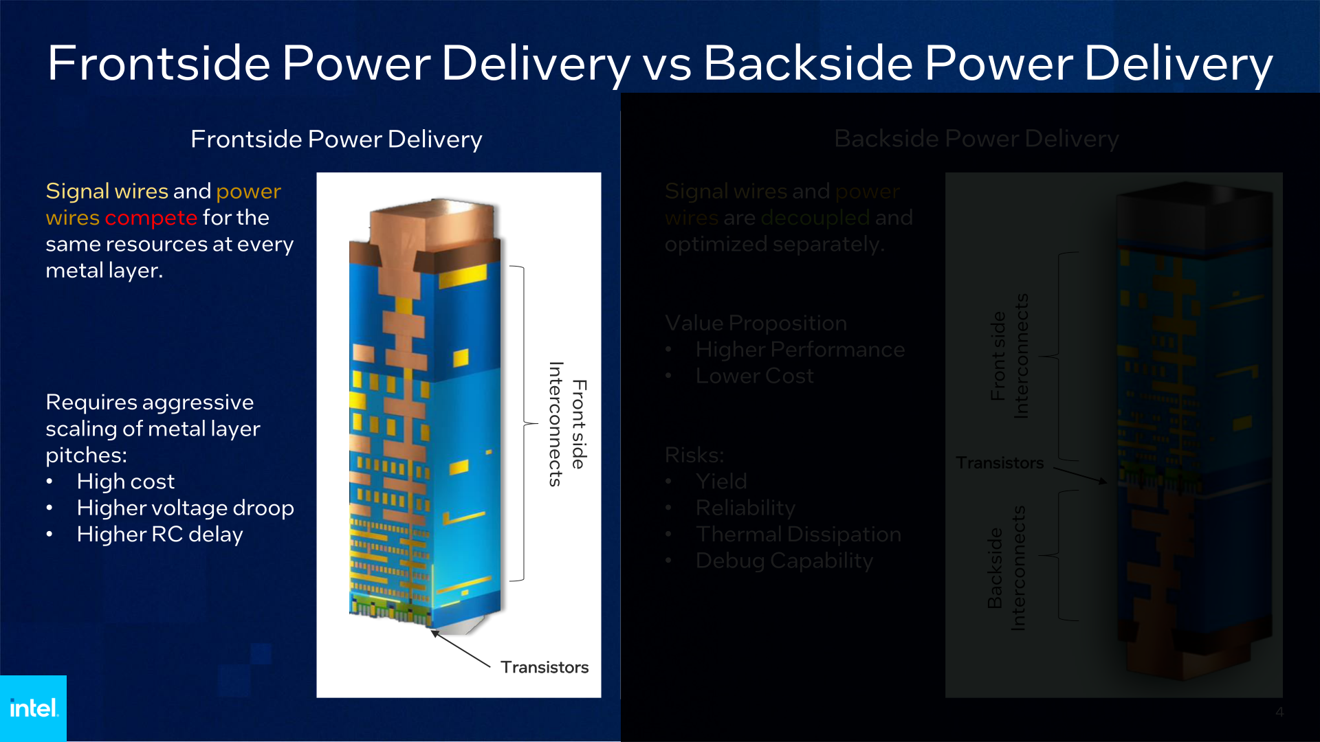
On the other hand, to fully understand how BS-PDN works, it is necessary to summarize how conventional (front-side) power delivery works and explore the many BS-PDN wafer constructions involved. The best place to start is to be able to contrast the changes.
The manufacturing process for modern front-side power delivery chips begins by etching the transistor layer M0. This is the smallest and most complex layer on the die and where precision tools such as EUV and multi-patterning are most needed. So it’s the most expensive and complex layer of the chip, and it has a significant impact on both how the chip is built and tested.
On top of that, additional metal layers are added in increasing size to carry all the necessary wiring between the transistors and the various parts of the processor (caches, buffers, accelerators), plus power coming in from above. wiring is also provided. stack. Intel compares this to making a pizza, which is crude but effective.
Modern high performance processor designs typically contain 10 to 20 metal layers. Especially in Intel 4 process, there are 16 logic layers with pitch from 30 nm up to 280 nm. And on top of that are two more “giant metal” layers just for power wiring and external connector placement.
Once the die is fully manufactured and polished, it is flipped over (called a flip chip) so that the chip can communicate with the outside world. This inversion puts all the connectors (power and data) on the bottom of the chip and the transistors are finally on the top of the chip. Once flip-chip manufacturing was mastered, debugging and cooling the chip became especially convenient, as debug tools had easy access to the most critical transistor layers. On the one hand, those hot little gates also became particularly close to the chip’s cooler, making it relatively easy for heat to flow in and out of the chip.
However, the drawback of front-side powering is that it means both power and signal lines are on the same side of the chip. Both wires have to descend well over 15 layers to reach the transistor, all the while competing for valuable space and causing interference with each other. Especially for power lines, this is especially troublesome. This is because the resistance along these lines causes the input power to drop in voltage, known as the IR drop/droop effect.
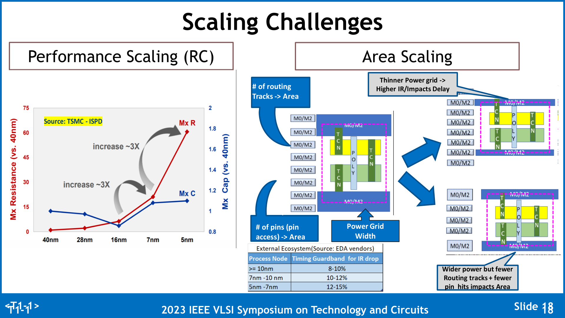
For most of the history of chip manufacturing, this hasn’t been a big deal. However, like many other aspects of chip manufacturing, this problem is becoming more pronounced as chip feature sizes shrink. There’s no hard and fast limit to front-side power delivery here, but given how difficult it is to shrink chips from generation to generation, the problem is too big (or rather too costly) to avoid. takes too long).
And that leads to the power supply on the back side. If having both signal and power on the same side of the chip causes problems, why not separate the two? That’s what I’m trying to solve by moving it to the other side of the wafer.
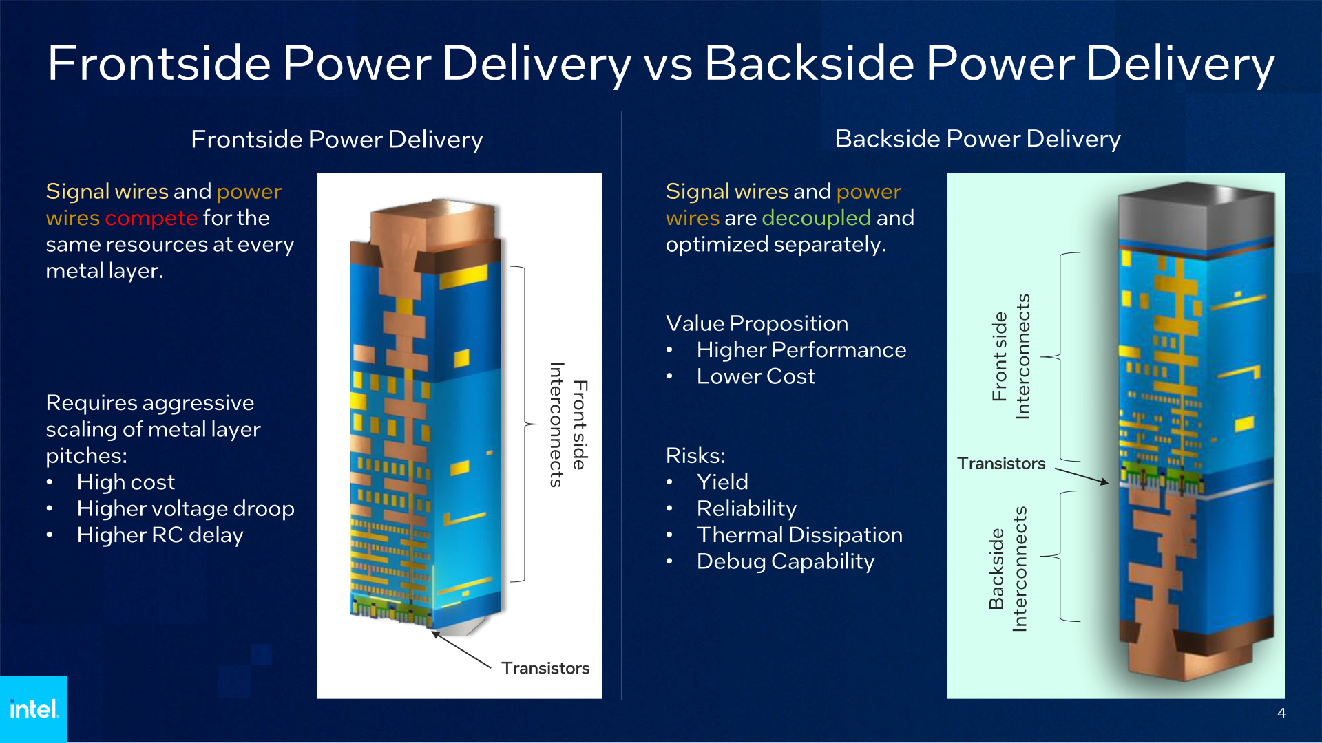
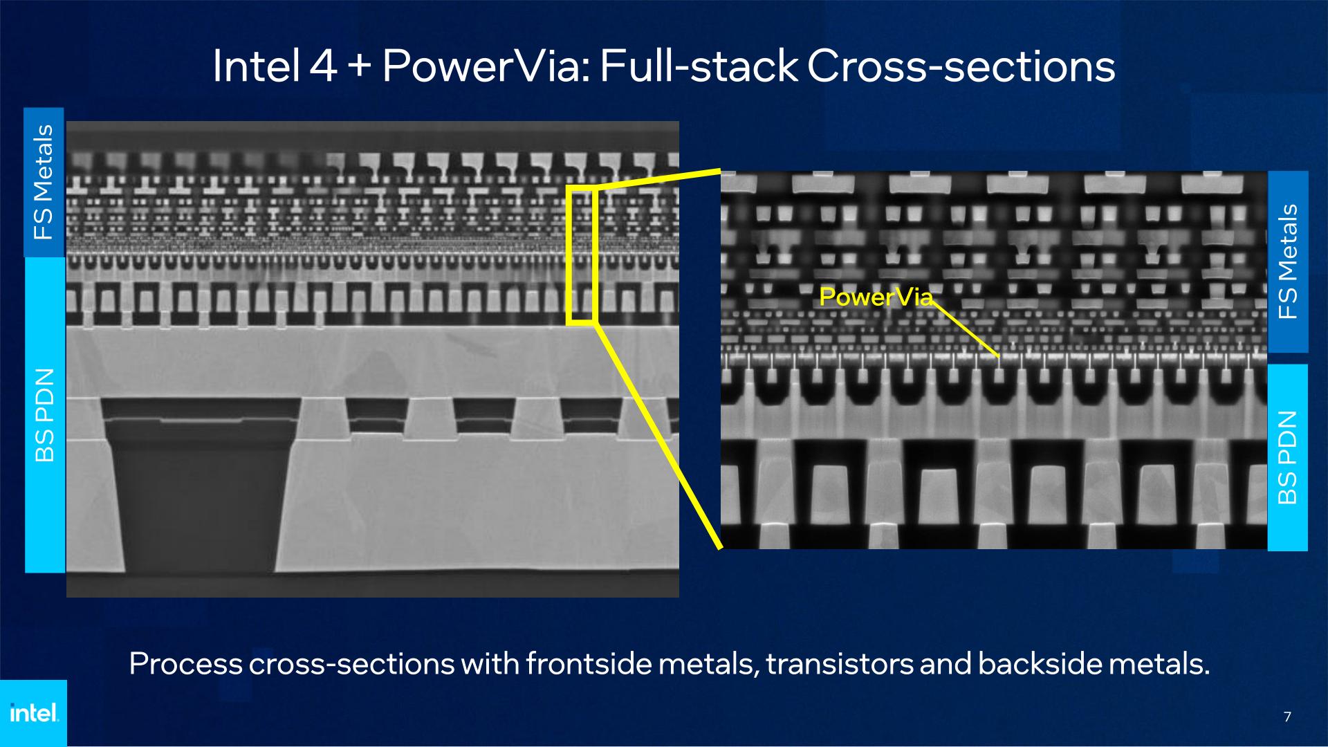
For Intel’s implementation of this concept in PowerVia, Intel literally flips the wafer and polishes away nearly all of the remaining silicon until it reaches the bottom of the transistor layer. At this point, Intel builds a metal layer for power delivery on the other side of the chip, similar to how they previously built a metal layer on the front of the chip. The end result is what is essentially a double-sided chip, with power on one side and signal on the other.
In theory (and also in Intel’s paper) moving to BS-PDN ultimately has some advantages. First and foremost, this has a major impact on the simplicity of chip construction. We’ll discuss Intel’s specific claims and findings later, but what’s particularly noteworthy here is that this allowed Intel to relax the density of his M0 metal layer. Instead of requiring a 30nm pitch on Intel 4, Intel’s test node for Intel 4 + PowerVia allowed a 36nm pitch. This directly simplifies the most complex and expensive processing steps across the chip and rolls them back to a size close to the Intel 7 process.
BS-PDN is also geared up to slightly improve chip performance. Shortening the route of power delivery to the transistor in a more direct manner helps counteract the IR droop effect, resulting in better power delivery to the transistor layer. Taking all of these power delivery wires out of the signal layer also improves signal layer performance, eliminates power interference, and gives chip designers more room to optimize their designs.
Otherwise, all these trade-offs are primarily about losing the aforementioned perks of building a frontside chip. The transistor layer is roughly in the middle of the chip, rather than on the edge. This means that traditional debugging tools cannot directly examine and test the transistor layers of the finished chip, and there are as many as 15 layers of signal lines between the transistor layers and the cooling services. increase. As the Intel paper carefully explains, these are not insurmountable challenges, but they were problems that Intel had to avoid in their designs.
Another trade-off in migrating to BS-PDN is manufacturability. Building a power layer on the backside of the die has never been done before and is more likely to cause problems. So not only does the power delivery have to work, it has to do so without significantly reducing chip yield or reducing chip reliability. But if all this goes well, the extra effort of building a power layer on the backside of the wafer will be well offset by the time and cost savings of not having to power from the front side. increase.
Intel Added Issues: Carrier Wafers and Nano TSVs
Backside power delivery networks will eventually become an industry standard feature, so we’ve been trying to focus less on Intel’s proprietary BS-PDN/PowerVia implementation. But now that you understand the basics of BS-PDN, there are some Intel-specific implementation details worth noting.
First and foremost, Intel uses carrier wafers as part of the build process to provide chip rigidity. After the front side of a PowerVia wafer has finished manufacturing, the carrier wafer that is glued to that front side is a dummy wafer that helps support the chips while Intel blows up on the other side. The double-sided chip manufacturing process polishes much of the remaining silicon wafer, so there isn’t much structural silicon to hold the whole. Even though this is silicon lithography, as Intel is joking lightly, by the end only a small amount of silicon will be left on the wafer.
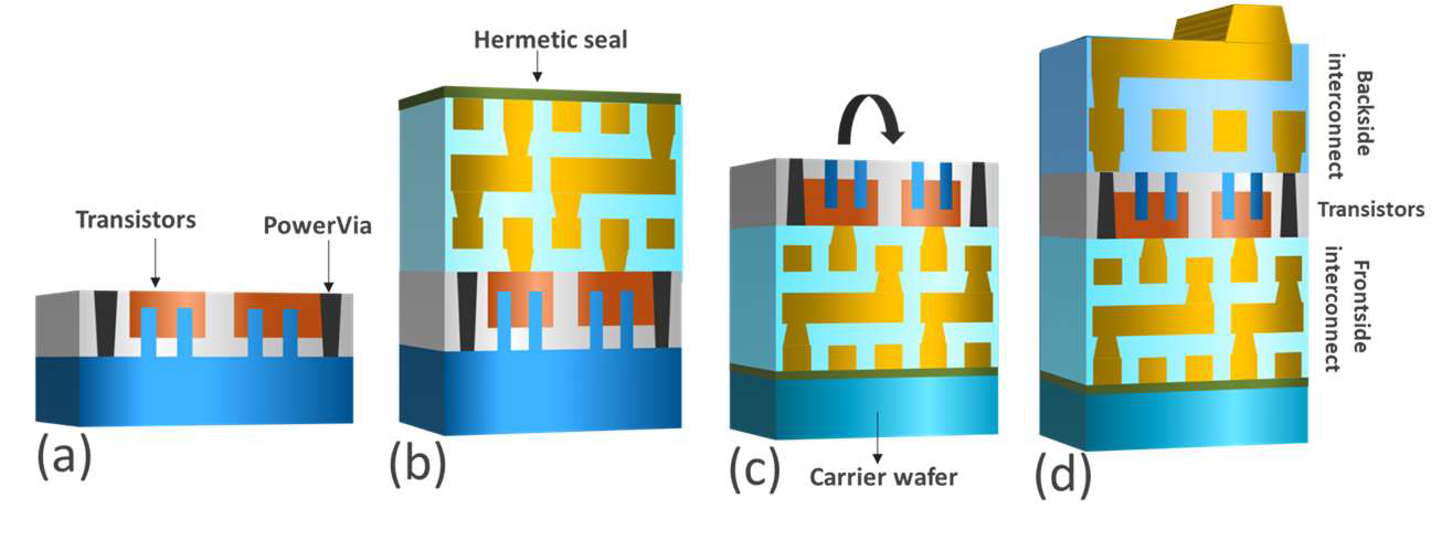
That carrier wafer remains part of the chip for the rest of its life. After chip fabrication is complete, Intel polishes the bonded carrier wafers to the required thickness. Notably, the carrier wafer is on the signal side of the chip, which means there is another layer of material between the transistors and the cooler. Intel’s tech to improve heat transfer takes this into account, but for his PC enthusiasts who are accustomed to having transistors on top of chips, this would be a breaking change.
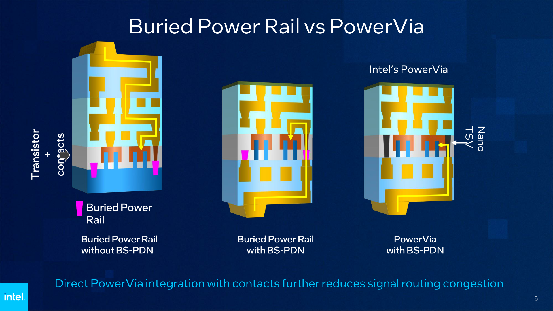
Another notable thing about Intel’s BS-PDN implementation is its use of TSVs for power routing. PowerVia has nanoscale TSVs (appropriately named Nano TSVs) in the transistor layer of the chip. This contrasts with the embedded power rails that industry pioneer IMEC is considering in his BS-PDN.
Importantly, while the power rail still has to pass over the transistor layer to deliver power, using a TSV allows power to be delivered more directly to the transistor layer. This is a technical advantage Intel hopes to take advantage of, as it eliminates the need to design and incorporate the wiring required for embedded power rails.


