
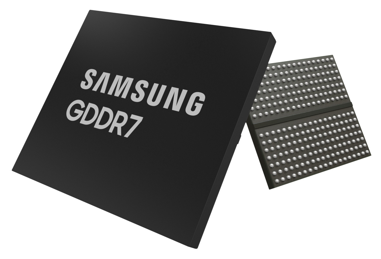
Samsung announced this evening that it has completed development of its first generation GDDR7 memory. The next version of the high-bandwidth memory technology in development across the industry is expected to hit the market in 2024, and Samsung is well-positioned to be one of the first memory vendors. The first-generation GDDR7 parts are expected to reach up to 32Gbps per pin in bandwidth, 33% more than the current best GDDR6 parts, and the company expects GDDR memory bandwidth to increase in the face of the technology’s adoption of PAM. We are about to achieve a significant increase. -3 signaling.
Samsung’s announcement comes amid a growing number of disclosures and announcements about upcoming versions of its widely used memory technology. The memory’s finished specifications have yet to be announced by JEDEC, but Samsung rival Micron has previously announced plans to launch its own GDDR7 memory in 2024, which is in line with Samsung’s current schedule. Same schedule. Meanwhile, EDA tools company Cadence released a fair amount of technical details earlier this year as part of its GDDR7 verification tool announcement, revealing that the memory uses PAM-3 signaling and reaches data rates of up to 36Gbps/pin. made it
With today’s announcement, Samsung became the first major memory maker to announce that it has completed the development of the first generation of GDDR7. Also, the company tends to announce this kind of memory relatively early in the launch process, well before the memory is ready for commercial production production, but this nonetheless is his GDDR7 development. It remains an important milestone in Device manufacturers can begin verification efforts against functional hardware. As for Samsung itself, the announcement gives the South Korean conglomerate a very visible opportunity to strengthen its leadership claim in the GDDR memory industry.
In addition to providing an update on the GDDR7 development process, Samsung’s announcement also provided some high-level technical details about the company’s first-generation GDDR7. However, this is by no means a technical detail, so “high-level” is the correct term. .
| Calculating GPU memory | |||||
| GDDR7 | GDDR6X | GDDR6 | |||
| black and white per pin | 32 Gbps (estimated) | 24 Gbps (as shipped) | 24Gbps (sampling) | ||
| chip density | 2GB (16GB) | 2GB (16GB) | 2GB (16GB) | ||
| Total B/W (256-bit bus) | 1024GB/s | 768 GB/s | 768 GB/s | ||
| DRAM voltage | ? | 1.35V | 1.35V | ||
| data rate | QDRs | QDRs | QDRs | ||
| signaling | PAM-3 | PAM-4 | NRZ (binary) | ||
| packaging | 266 FBGA | 180FBGA | 180FBGA | ||
According to Samsung’s announcement, the data rate is expected to reach 32Gbps/pin. This is 33% higher than his 24Gbps data rate, which the company’s top GDDR6 product can currently achieve. Samsung and Cadence have previously clarified that they expect GDDR7 memory to eventually reach 36Gbps/pin, but similar to the development of GDDR6 (which is a whopping 50% faster than GDDR6), this may take multiple generations of the product.
Interestingly, this is much closer to the predicted limits of GDDR7 than we have seen in previous generations of memory technology. GDDR6 he launched at 14Gbps and eventually he scaled up to 24Gbps, but Samsung wants him to start at 32Gbps. But at the same time, GDDR7 will be a smaller generation leap than GDDR6 and his GDDR5. GDDR7 is only a 50% increase in the signaling bandwidth of the memory technology over the previous generation, instead of doubling, due to the switch from NRZ (2-state) signaling to PAM-3 (3-state) signaling.
Also note that the fastest GDDR6 memory used in used video cards today only runs at 20Gbps. His 24Gbps GDDR6, which is Samsung’s own, was announced over a year ago, but is still only a “sample” at this point. So even though there are many other products using GDDR6, the effective increase in bandwidth for video cards in 2024/2025 could be even greater, depending on the speed grades available at the time. there is.
In terms of capacity, Samsung’s first GDDR7 chips are 16Gb, matching the existing density of today’s top GDDR6(X) chips. Therefore, assuming the same memory bus width, the memory capacity of the final product will not change much from the current product. Overall DRAM density growth has slowed in recent years due to scaling issues, and GDDR7 is not immune to that.
Samsung also claims that its GDDR7 technology is “20% more power efficient than existing 24Gbps GDDR6 DRAMs”, but that’s a loose claim with a few details. DRAM power efficiency is usually measured in bits (picojoules/bits/pJpb), so we interpret this to be the number Samsung is referring to in its claims. However, it remains unclear whether that measurement was done at his 24Gbps (equal bandwidth) or 32Gbps.
Either way, the good news is that Samsung’s GDDR7 is set to deliver tangible improvements in energy efficiency. However, the memory technology is only 20% more energy efficient with up to 33% more bandwidth. This means that the memory’s absolute power consumption has increased compared to the previous generation.. Assuming Samsung’s energy efficiency numbers are for GDDR7@32Gbps and GDDR6@24Gbps, the total energy consumption will increase by about 7%. Otherwise, for equal bandwidth, the increase in power consumption over full bandwidth could be even greater, depending on what Samsung’s voltage/frequency curve looks like.
Broadly speaking, this is the same result we saw with the introduction of GDDR6(X). Despite improvements in energy efficiency, the overall power consumption has increased with each generation as energy efficiency improvements have not kept up with bandwidth demand. . None of this is unexpected, but it does mean that proper cooling will become even more important for GDDR7 memory.
However, for customers with stringent power/cooling needs, Samsung has also announced that it will offer a lower voltage version of its GDDR7 memory. The company hasn’t revealed the nominal voltages for GDDR7 or its low-voltage variants, but Samsung is expected to use the same chips running at lower clocks, as well as low-voltage GDDR6, in exchange for lower operating voltages.
Also, Samsung’s disclosure doesn’t provide any information about the manufacturing process it uses to make its new memory. The company’s latest GDDR6 uses his D1z process, while recent DDR5 memory announcements from Samsung use 12nm (D1b?). Even if we don’t know the specific node used, Samsung is almost certainly using the new node for his GDDR7. This means that at least some of the 20% energy efficiency improvement from GDDR7 will come from the new nodes, rather than the inherent efficiency gains from GDDR7.
However, Samsung is certainly working on them as well. The details are pretty brief, but the company says that the GDDR7 memory uses “IC architecture optimizations” to keep power and heat down.
Electronics manufacturing aside, the final big innovation with Samsung’s GDDR7 is clearly physical: epoxy. Clearly considering the high heat load already generated by his existing GDDR memory running at top speed, Samsung’s press release stated that a new epoxy molding compound designed to conduct heat better ( EMC) for his GDDR7. Overall, Samsung claims that the thermal resistance he has reduced by 70% compared to GDDR6 memory. This should help a good cooler pull enough heat out of the memory chips, despite the overall increased heat output.
In summary, with the initial development of GDDR7 memory complete, Samsung is now moving forward with validation testing with partners. The company says it plans to work with a major customer to do a validation this year. However, at this time, the company has not announced when mass production of the new memory will begin.
Given the timing of Samsung’s (and Micron’s as well) announcements, it seems likely that the first market for GDDR7 will be AI and network accelerators, rather than video cards for which GDDR7 is named. Both AMD and NVIDIA are only a quarter of the way through their current architecture release cycle, so it’s possible that neither will be ready to use his GDDR7 in 2024 when GDDR7 is ready. I have. Instead, other users of his GDDR memory, such as networking products and high-performance accelerators, are likely to be the first to use the technology.


