
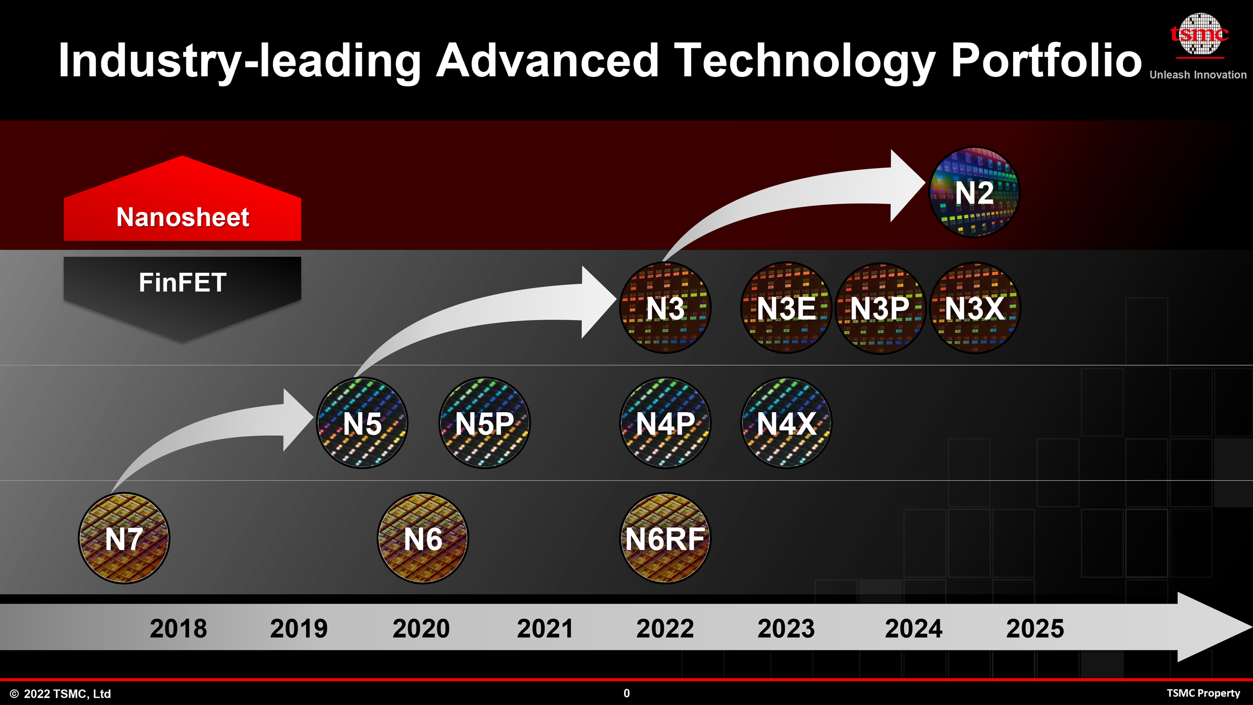
When TSMC first introduced N2 (2 nm class) process technology earlier this month, the company showed how to build new nodes behind two new state-of-the-art fab technologies (gate all-around transistors and rear power rails). I outlined it. .. But as we learned from last week’s EU symposium, TSMC’s plans are a bit more subtle than originally announced. Unlike some rivals, TSMC does not implement both technologies in the initial version of the N2 node. Instead, the first iteration of N2 implements only the gate all-around transistor and provides backside power with a newer version of the node.
So far, TSMC has mentioned two distinctive features of N2. It is a nanosheet gate all-around (GAA) transistor and a backside power rail. GAA transistors have two unique advantages over FinFETs. The GAAFET channels are horizontal and all four sides are surrounded by gates, solving many of the leak current related challenges. On the other hand, the power rails on the back side improve the power supply to the transistors, improve performance, and reduce power consumption.
But after all, TSMC does not plan to start with both nanosheet GAA transistors and backside power rails in the early generations of N2 process technology. As the company announced at last week’s EU symposium, the first generation N2 will only have gate all-round transistors. Backside power supply, on the other hand, will be provided later in a more advanced implementation of the N2.
At this point, the company hasn’t said much about why it doesn’t deploy backside power supplies as part of the first N2 node. However, when discussing branching, TSMC pointed out that the backside power supply would eventually add additional process steps. This seems to be trying to avoid it the first time I try GAAFET.
The lack of backside power supply in the original version of the N2 manufacturing technology probably explains a fairly modest performance improvement for the N2 when compared to the N3E node... For high performance computing (CPU, accelerator, etc.), a 10% to 15% performance improvement with the same power and complexity does not seem to be impressive, but a 25% to 30% power reduction with the same speed and complexity. Can be seen very suitable for mobile applications.
| Improved PPA advertised for new process technology Data published during conference calls, events, press briefings and press releases |
|||||
| TSMC | |||||
| N5 vs N7 |
N3 vs N5 |
N3E vs N5 |
N2 vs N3E |
||
| Power | -30% | -25-30% | -34% | -25-30% | |
| performance | + 15% | + 10-15% | + 18% | + 10-15% | |
| Chip density * | ?? | ?? | ~ 1.3X | > 1.1X | |
| Volume Manufacturing |
Second quarter of 2022 | H2 2022 | 2nd to 3rd quarter of 2023 | H2 2025 | |
* The chip density published by TSMC reflects a “mixed” chip density consisting of 50% logic, 30% SRAM, and 20% analog.
Given that TSMC always offers multiple versions of its node, it’s not surprising that TSMC has several variants planned for N2. Nevertheless, it’s a bit strange to see TSMC go a long way on the backside power supply.
In contrast to its competitors, this is a significant difference from how rival Intel handles its own GAAFET / rear power migration in the Intel 20A process. Intel plans to introduce GAA Ribbon FET transistors and PowerVia interconnects together in mid-2024. This goes as far as creating an internal pseudonode just to focus on RibbonFET development. TSMC, on the other hand, takes a more cautious approach to risk and innovation. Not only can TSMC move slowly, but it is also a better approach to the need for TSMC to provide something more consistent and consistent in the past. Update of that fab product.
And, for a few years now, it’s interesting to see what this means for the competitiveness of TSMC’s first-generation N2 nodes. Is a GAAFET process without backside power supply a significant disadvantage? According to the current schedule, the answer will be available in late 2025, when TSMC’s first N2 node will enter mass production (HVM).


