
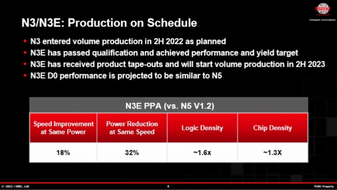
In addition to several new announcements on its 2nm process node plans, TSMC also released an update on its N3 family process technology progress and roadmap at its 2023 North American Tech Symposium today. TSMC’s last-generation FinFET-based process node, the N3 family, will be in some form or another for years to come as the highest-density node available to customers who don’t need the cutting-edge of his GAAFET-based process. expected to continue to exist.
TSMC’s big roadmap update on the N3 front involved the N3P and its high-performance variant, the N3X. As announced today by TSMC, N3P will be an optical shrink of N3E, offering enhanced performance, reduced power consumption and increased transistor density compared to N3E while maintaining compatibility with N3E’s design rules. Realize Meanwhile, N3X delivers extreme performance at 3nm-class densities, offering higher clock speeds for high-performance CPUs and other processors.
N3E: 3nm for everyone on schedule
As a quick refresher, TSMC’s N3 (3nm class) process technology family includes a baseline N3 (aka N3B), a relaxed N3E with reduced cost, an N3P with enhanced performance and chip density, and a higher voltage tolerance. It consists of several variants including the equipped N3X. Last year, the company also talked about his N3S, which maximized transistor density, but this year has been tight-lipped about this node, not mentioned anywhere in the slides.
TSMC’s vanilla N3 node will feature up to 25 EUV layers, with TSMC using EUV double patterning on some of them to achieve higher logic and SRAM transistor densities than N5. EUV steps are generally expensive, and EUV double patterning pushes those costs even further.
| Advertised PPA improvements for new process technology Data presented in conference calls, events, press briefings and press releases |
|||
| TSMC | |||
| N3 versus N5 |
N3E versus N5 |
||
| Power | -25-30% | -32% | |
| performance | +10-15% | +18% | |
| logic area
Discount*% Logic density* |
0.58 times
-42% 1.7 times |
0.625x
-37.5% 1.6 times |
|
| SRAM cell size | 0.0199µm² (-5% vs N5) | 0.021µm² (same as N5) | |
| Volume manufacturing industry |
Late 2022 | Second half of 2023 | |
The majority of TSMC’s clients interested in 3nm-class processes are expected to use the eased N3E node, which TSMC says is on schedule and meeting performance targets. N3E uses up to 19 EUV layers and does not rely on EUV double patterning at all, thus reducing complexity and cost. The trade-off is that N3E offers lower logic density than N3 and the same SRAM cell size as TSMC’s N5 node, making it less attractive to customers pushing for density/area improvements. Overall, N3E promises a wider process window and improved yield. These are two important metrics in chip manufacturing.
“N3E is superior to N3 in terms of yield and process complexity. [wider] process window,” said Kevin Zhang, vice president of business development at TSMC.
N3P: high performance, high transistor density
Following N3E, TSMC continues to optimize transistor density for the N3 family with N3P. N3P builds on N3E by offering improved transistor characteristics. A sophisticated process node allows a chip designer to get a 5% performance boost with the same leakage or a 5%-10% reduction in power with the same clock. The new node will also increase transistor density by 4% in a “mixed” chip design, which TSMC defines as a chip composed of 50% logic, 30% SRAM, and 20% analog circuitry.
As part of the discussion on N3P, TSMC highlighted that the increased density was achieved by tuning the scanner’s optical performance. all N3P will be an attractive node for SRAM-intensive designs.
“N3P improves performance. It’s 5% better, at least 5% better than N3E,” Zhang explains. Also, a 2% optical shrink increases transistor density by a factor of 1.04. ”
| Advertised PPA improvements for new process technology Data presented in conference calls, events, press briefings and press releases |
|||||
| TSMC | |||||
| N3 versus N5 |
N3E versus N5 |
N3P versus N4E |
N3X versus N3P |
||
| Power | -25-30% | -32% | -5% ~ 10% | taller than | |
| performance | +10-15% | +18% | +5% | +5% Fmax @ 1.2V |
|
| chip density | ? | ? | |||
| SRAM cell size | 0.0199µm² (-5% vs N5) | 0.021µm² (same as N5) | ? | ? | |
| Volume manufacturing industry |
Late 2022 | Second half of 2023 | Second half of 2024 | 2025 | |
N3P is an optical shrink of N3E, thus preserving N3E design rules and allowing chip designers to quickly reuse N3E IP in new nodes. As a result, N3P is predicted to become one of TSMC’s most popular N3 nodes, so IP design firms such as Cadence and Synopsys are providing various IPs for this process technology to compete with the existing N3E. We expect you to enjoy the compatibility in your process. According to TSMC, the N3P will hit the market in the second half of 2024.
N3X: Highest Performance and Density
Finally, for developers of high-performance computing applications such as CPUs and GPUs, TSMC has offered the X family of high-voltage, performance-focused nodes for the past several generations. As revealed at last year’s event, the N3 family will get its own X variant with the aptly named N3X node.
Compared to N3E, N3X is projected to offer at least 5% higher clock speeds compared to N3P. This is achieved by making the node more tolerant to higher voltages, allowing chip designers to increase clock speeds at the expense of higher overall leakage.
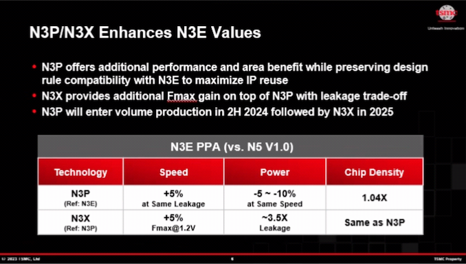
TSMC claims the N3X will support voltages of (at least) 1.2v. This is a fairly extreme voltage for a 3nm class manufacturing process. The cost of leakage is significant, as TSMC predicts 250% more power leakage than his more balanced N3P node. This is why the N3X is really only available in his HPC class processors and chip designers need to be very careful to check the most powerful (and power hungry) chips. I am emphasizing that
In terms of transistor density, N3X offers the same density as N3P. TSMC has not commented on whether they will also maintain design rule compatibility with N3P and N3E, so it will be interesting to see what happens there.
The last N3 family node on TSMC’s current roadmap, the company says the N3X will be production ready in 2025.


