
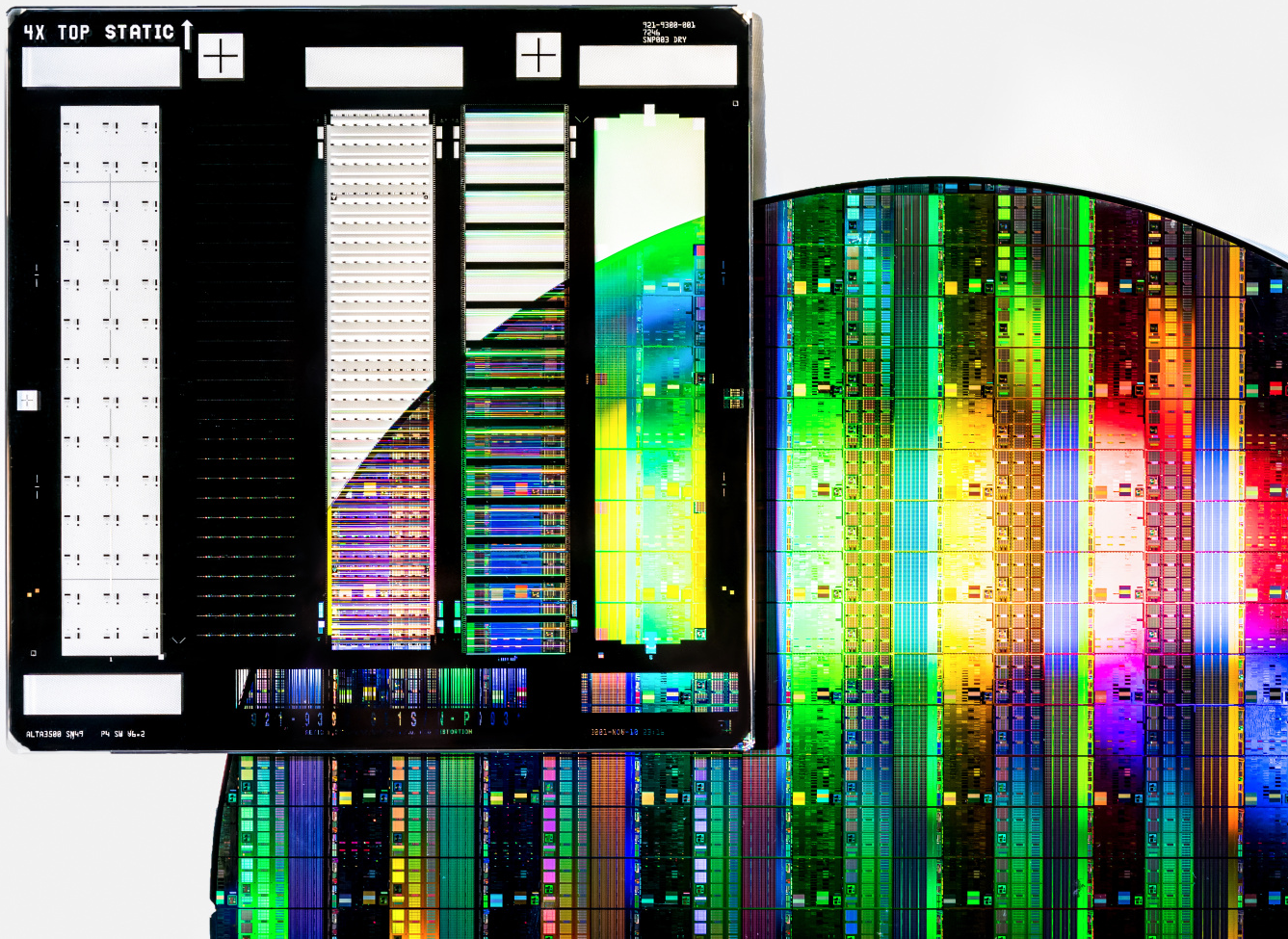
Manufacturing chips using state-of-the-art process technology requires more computing power than ever before. To meet the requirements of the 2nm node and beyond, Nvidia is rolling out a cuLitho software library that uses the company’s DGX H100 system based on the H100 GPU, delivering performance available to mask shops within reasonable power consumption. promises to improve 40x.
Modern process technologies are pushing wafer fab equipment to its limits, often requiring finer resolution than is physically possible. This is where computer lithography comes into play. A major goal of computational lithography is to improve the resolution achievable in photolithographic processes without changing tools. To do so, CL employs algorithms that simulate the production process and incorporates key data from ASML’s equipment and shuttle (test) wafers. These simulations help improve pellicles (photomasks) by intentionally altering patterns to counteract the physical and chemical effects that occur throughout the lithography and patterning steps.
Computational lithography techniques include Resolution Enhancement Technology (RET), Inverse Lithography Technology (ILT, a method that uses non-rectangular features on the photomask to reduce manufacturing variability), and Optical Proximity Correction (OPC, a technique that improves photolithography. ) And so on. correction of image inaccuracies due to diffraction or process-related effects), and source mask optimization (SMO). They are all widely used in today’s fabs.
On the other hand, computationally expensive techniques such as inverse lithography techniques and source mask optimization are specific to a particular design. To ensure adequate resolution and avoid yield-limiting hot spots, each chip must be implemented individually. Pellicle synthesis using RET, ILT, OPC, and SMO involves the use of computational lithography. Computational complexity increases as nodes get thinner, and with each modern chip using dozens of pellicles, computational power becomes the bottleneck for mask shops. For example, Nvidia’s H100 uses his 89.
According to Nvidia, computational lithography currently consumes tens of billions of CPU hours each year, which is a huge power drain. On the other hand, highly parallelized GPUs like Nvidia’s H100 promise higher performance at lower cost and power consumption. Notably, Nvidia has 500 DGX H100 systems with 4000 H100 GPUs (consuming 5 MW of power) and 500 DGX H100 systems with computational lithography software using cuLitho compared to TSMC’s 40,000 GPUs consuming 35 MW. It states that it can provide the performance of CPU-based systems. I will use it today. The company further says that when mask makers start relying on GPU-accelerated computational lithography, they can produce three to five times as many pellicles per day with one-ninth the power they use today. increase. But this gives you a basic understanding of where the company wants to go.
“With lithography pushing the limits of physics, the introduction of cuLitho by Nvidia and collaboration with our partners TSMC, ASML and Synopsys will help fabs increase throughput, reduce carbon footprint and We can lay the groundwork for the rest.”

While the performance targets set by Nvidia are impressive, the cuLitho software library for computational lithography must be built into software provided by ASML, Synopsys, and TSMC, which is commonly used by partners among mask shops. be careful not to For current generation lithography (think 7nm, 5nm and 3nm class nodes), mask shops are already using CPU-based computational lithography solutions and will continue to do so for at least some time. It’s a schedule. This is probably why Nvidia is discussing computational lithography efforts in the context of the next generation of his 2 nm class node and beyond. On the other hand I would expect foundries and mask shops to try to introduce at least his Nvidia’s cuLitho in some of his upcoming 3 nm class nodes to improve yield and performance Makes sense. For example, TSMC will begin certifying his cuLitho in mid-2023, so the platform is expected to be available to the company’s customers from 2024.
“Computational lithography, especially optical proximity correction (OPC), is pushing the boundaries of computational workloads on state-of-the-art chips.Synopsys Chief Executive Officer Earl de Geus said:Working with our partner Nvidia to run the Synopsys OPC software on the cuLitho platform has resulted in significant performance improvements of weeks to days! continues to make progress.“
In an official statement from NVIDIA, “Fab process changes often require OPC revisions, creating bottlenecks.” “cuLitho not only helps eliminate these bottlenecks, but also enables new solutions and innovative techniques such as curved masks, high NA EUV lithography and sub-atomic photoresist modeling required for new technology nodes.“
The additional computational power available for computational lithography applications is particularly useful for next-generation production nodes using high-NA lithography scanners, allowing the use of ILT, OPC, and SMO to take into account the physical properties of lithography scanners and resists. oblige. It guarantees good yields, low variability (that is, predictable performance and power consumption), and predictable costs. On the other hand, the computational costs of RET, ILT, OPC and SMO will inevitably increase beyond 2 nm, so it looks like Nvidia will introduce his cuLitho platform at the right time.


