
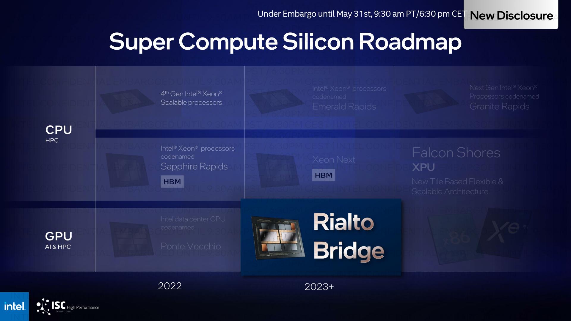
At ISC HighPerformance 2022 in Hamburg, Germany this week, Intel will use a face-to-face version of the event for the first time in three years to update the status of its high-performance / supercomputer silicon plans. The big news of this year’s show is that Intel has nominated a successor to the Ponte Vecchio accelerator. This is what the company is currently disclosing as Rialto Bridge.
Previously listed on Intel’s roadmap as “Ponte Vecchio Next,” Intel’s GPU team is the successor to Ponte, even though the first major installation of Ponte itself (Aurora supercomputer) is still up and running. We have been developing the machine in the pipeline. As part of the company’s three-year roadmap to the integration of CPUs and accelerators into the FalconShores XPU, Rialto Bridge, if allowed to flirt, bridge The gap between Ponte and Falcon. It offers the evolution of Ponte’s design using new technologies and manufacturing processes.
Intel doesn’t provide a complete technical breakdown early in the process, but broadly speaking, Intel not only talks a bit about the spec, but also removes all suspicions of Ponte’s successor. Provides rendering of future chips. It shows that it consists of dozens of tiles / chiplets with the same layout as Ponte. The biggest change Intel is talking about today is to increase the total number of Xe computing cores from 128 in Ponte to up to 160 in Rialto Bridge. Probably by increasing the number of Xe cores in each compute tile.
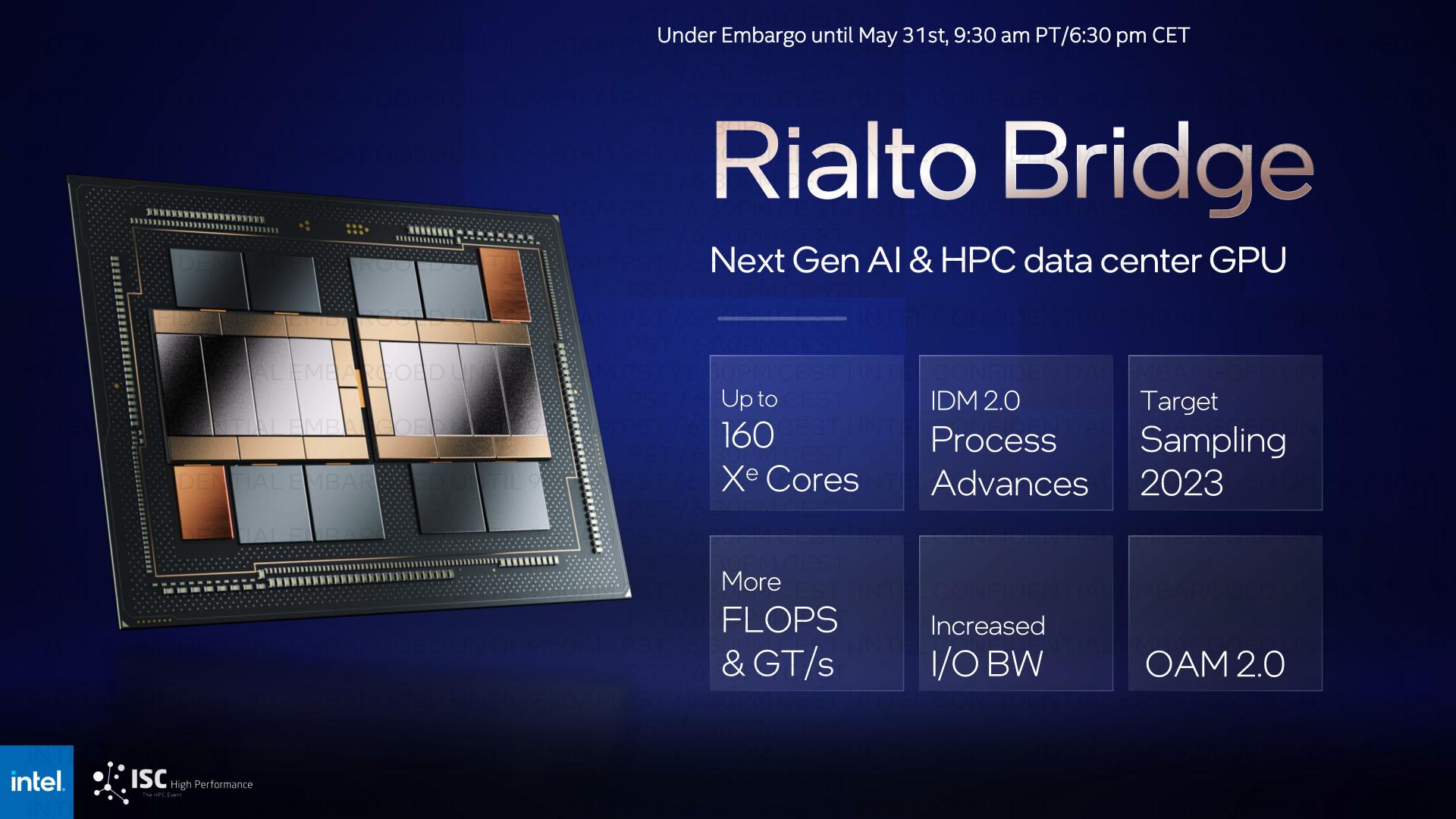
Without specific manufacturing details, Intel will use the new manufacturing node, at least with Rialto replacing the current combination of TSMC N7 (Link Tile), TSMC N5 (Compute), and Intel 7 (Cache). I have confirmed that it will be built. & Base) Parts. The Intel 4 process will be online this year, so it makes sense to use it to upgrade the base and cache. Ideally, Intel wants to jump to the process node of the compute tile as well. Perhaps we will take this opportunity to move production of these tiles to Intel 4, but we will not count TSMCN4 either.
That said, Rialto has one notable difference from Ponte when it comes to computing cores, because there is a risk of reading too much for a single renderer. Ponte used a pair of computing cores with cache tiles in between, but Rialto seems to be using a monolithic slab at first glance. This means that Intel has chosen to integrate Rambo cache with compute tiles on-die and is willing to create fewer, larger compute tiles. This gives some credibility to the idea that Intel is taking over the production of computing tiles (because we have already created the cache tiles), but we need to check what Intel will announce later. ..
Interestingly, Intel has also promised to increase Rialto’s I / O bandwidth, which is also a very high level (and unspecified) detail. This is on-chip bandwidth rather than off-chip bandwidth, or Intel’s, as Ponte was already one of the first products to ship with a PCIe 5.0 connection and the PCIe 6.0 hardware is still a bit off. XeLink interconnect, which may be related to the amount of bandwidth available between the accelerators.
The HBM3 is also a shoe-in for Intel’s next-generation accelerators, given that accelerators are already shipping this year. HPC accelerators run mostly live and die based on memory bandwidth, so it’s likely that Intel first considered it at Rialto. Also, memory bandwidth is often measured with giga transfers, which matches Intel’s nasty expression “More GT / s”.
Finally, Intel states that Rialto is based on a new version of the Open Accelerator Module (OAM) socket specification. This is especially noteworthy as the next version of OAM has not yet been announced. Without the details, the biggest differentiator seems to be the supported power. While modules can consume up to 700 watts in OAM 1.x, Intel is discussing consuming up to 800 watts in Rialto modules. This is in line with the increased power consumption of the highest performance versions of next-generation HPC accelerators, for better or for worse, and is a major factor in the transition of high-end hardware to liquid and immersion cooling.
| Calculate GPU Accelerator Comparison | |||
| AnandTech | Intel | Intel | NVIDIA |
| product | Rialto Bridge | Ponte Vecchio | H100 80GB |
| Architecture | Xe-HPC | Xe-HPC | Amps |
| Transistor | ?? | 100 B | 80 B |
| Tiles (including HBM) | 31? | 47 47 | 6 + 1 spare |
| Computation unit | 160 | 128 128 | 132 132 |
| Matrix core | 1280? | 1024 | 528 |
| L2 / L3 | ?? | 2 x 204MB | 50MB |
| VRAM capacity | ?? | 128 GB | 80 GB |
| VRAM type | HBM3? | 8 x HBM2e | 5 x HBM3 |
| VRAM width | ?? | 8192 bits | 5120 bits |
| VRAM bandwidth | ?? | ?? | 3.0 TB / s |
| Chip-to-chip total BW | ?? | 64 x 11.25 GB / s (4×16 90G SERDES) |
18 x 50 GB / s |
| CPU coherency | yes | yes | Use NVLink 4 |
| Manufacturing | ?? | Intel 7 TSMC N7 TSMC N5 |
TSMC N4 |
| Form factor | OAM 2.0 (800W) | OAM (600W) | SXM4 (400W *) |
| Release date | Mid 2023 (sampling) | 2022 | 2022 |
| * Some custom deployments can be up to 600W | |||
Overall, Intel aims to use Rialto bridges to improve “application-level” performance by 30%. This is not a big profit at first, but it is also a part that will be released about a year after the original Ponte Vecchio. A 25% increase in the number of Xe cores means that most of this performance improvement needs to be achieved by additional hardware rather than clock speed changes, but Intel theoretically It’s not too surprising if the Rialto paper specs are still a bit rich, as they quote actual performance expectations rather than throughput. Intel also promises that Rialto should be more efficient than Ponte. This is a face value claim as performance should go faster than power consumption.
According to Intel’s roadmap, the Rialto Bridge will begin sampling in mid-2023. Given that Intel is having a hard time getting the Ponte Vecchio out on time, you can’t get it without Aurora. This is a surprisingly fast turnaround time for Intel. But at the same time, these are pipeline designs with very strong architectural similarities, so ideally Intel wouldn’t experience as many toothy problems as Ponte in real life. But as always, as Intel approaches the next accelerator offering, we’ll see what’s really going to happen next year.
All roads lead to Falcon Shores
With the addition of Rialto Bridge to Intel’s HPC plan, the company’s current silicon roadmap is as follows:
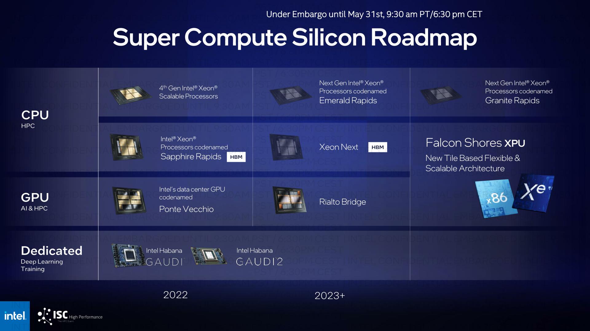
Both Xeon and HPC accelerator lines with HBM will be integrated with Intel’s first flexible XPU, Falcon Shores, in 2024. Falcon Shores was first unveiled at Intel’s Winter Investors Conference earlier this year and is Intel’s first to draw logical conclusions on high-performance CPU and GPU tiles by enabling configurable numbers of each tile type. It will be a product of. As a result, Falcon Shores is the successor to both Intel’s HPC CPUs and HPC GPUs, as it covers not only mixed CPU / GPU designs, but also (relatively) pure CPU and GPU designs.
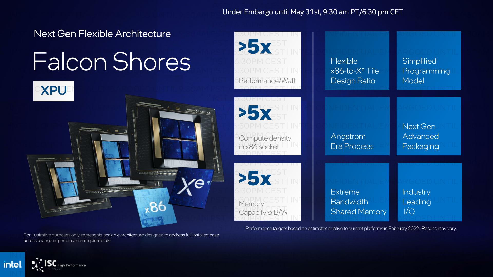
At today’s event, Intel does not provide details on Falcon Shores. That’s why the company aims to increase everything from energy efficiency to computational density to memory bandwidth by a factor of five. In addition to relying on planned packaging and shared memory technology, it’s still unclear how they’re trying to achieve that. However, this update gives you a better idea of where Falcon Shortes fits into Intel’s product roadmap by seeing how the current HBM-Xeon and Xe-HPC products integrate.
Ultimately, Falcon Shores remains Intel’s power play in the HPC industry. The ability to provide a tightly integrated (but tiled and flexible) experience for everyone using a single API gives the HPC market an edge over traditional GPU-based accelerators. I’m sure it’s also excellent. And if those plans can be realized, 2024 is becoming a very interesting year in the high performance computing industry.


