
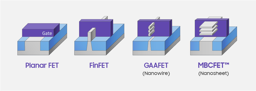
Samsung’s Foundry Group concludes its multi-year development process and announced this morning that the company has officially launched production on its first 3nm chip production line. Samsung’s 3nm process is the industry’s first commercial production process node using gated all-around transistor (GAAFET) technology, marking a major milestone in silicon lithography and making significant efforts for Samsung to compete with TSMC. May boost to.
Relatively simple Announcement from Samsung, Announced on the last day of the second quarter, Samsung has begun production of chips on a GAAFET-enabled 3nm production line. The company does not disclose the specific version of the node used here, but based on the previous Samsung roadmap, this is arguably Samsung’s first 3GAE process, basically the Samsung family. The earliest process node in the. According to Samsung, the line will initially be used to manufacture chips for “high performance, low power computing”, with mobile processors coming later. Samsung hasn’t announced a specific 3nm chip today because Samsung’s early process nodes are traditionally reserved for internal use by the company, but we see Samsung LSI announcing a 3nm SoC. Is just a matter of time.
Samsung has mostly remained silent about this year’s 3nm / GAAFET progress. The last important news I heard from the company about this was the company’s foundry forum event a few months ago, when the company repeated plans to produce 3GAE by the end of 2022. Given the previous silence and cutting-edge nature, there was concern that 3GAE would be delayed after 2022 when it comes to technology. This adds to the delay that technology is out of the original 2021 launch window, but with today’s announcement, Samsung seems to want to rest.
That said, the devil is detailed in these announcements about what is said and what is not said. Literally, today’s announcement from Samsung does not specifically mention the traditional milestone of “mass production” when process nodes became commercially available. So just saying that 3nm is in production leaves a lot of room for the company in terms of the number of chips they can produce and their yield. Since the company manufactured test chips in 2021, the problem is more subtle than just launching a fab, so the line between PR and commercialization is ambiguous, to say the least.
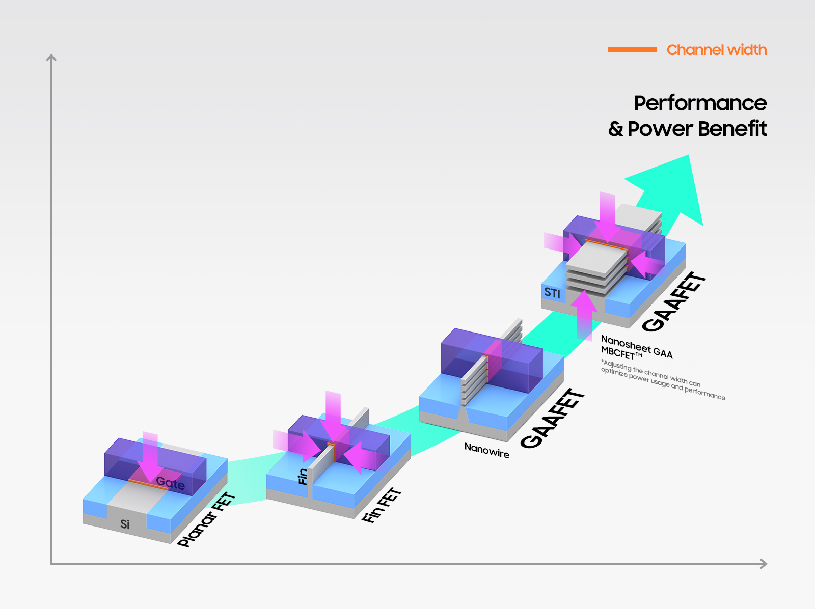
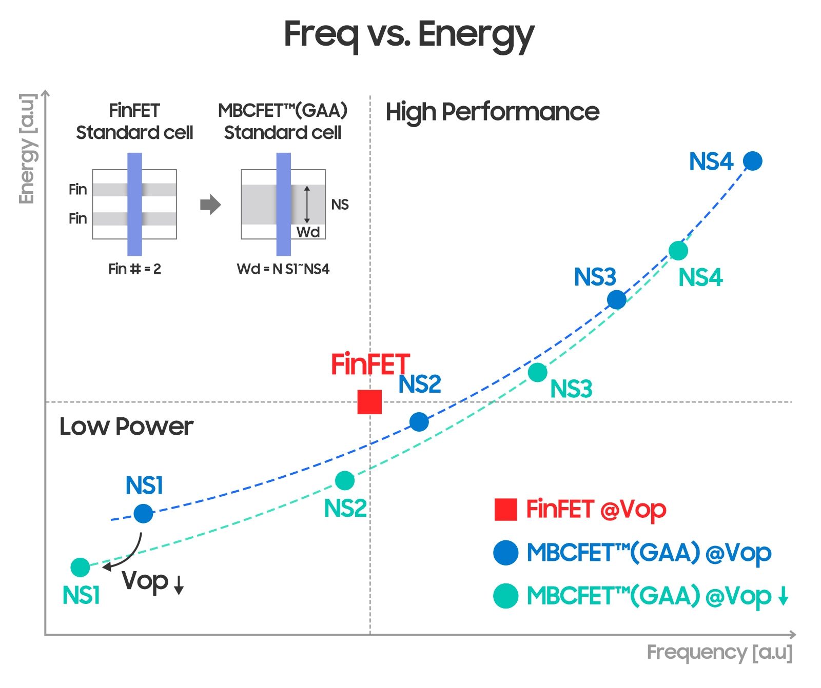
Still, today’s announcement is an important moment for Samsung, which has been working on 3nm / GAAFET technology since before 2019, when the technology was first announced. A particular flavor of Samsung’s GAA transistor technology is the multi-bridge channel FET (MBCFET), which is a nanosheet-based implementation. Nanosheet-based FETs are highly customizable, and nanosheet width is an important indicator in defining power and performance characteristics. The wider the width, the higher the performance (higher power). As a result, transistor designs focused on low power can use smaller nanosheets, while logic that requires higher performance can use wider sheets.
In addition to today’s production announcement, Samsung also offers some updated size and performance figures comparing the 3GAE to older nodes. Officially, 3GAE reduces power consumption by 45%, improves performance by 23% and overall feature size by 16% compared to Samsung’s 5nm process (the company doesn’t specify any flavor). Reduce. These numbers are significantly different from Samsung’s previous (2019) numbers comparing the technology to Samsung’s 7LPP nodes. Given the baseline changes, it’s not clear at this point whether 3GAE is responding to Samsung’s first claim or having to step back a bit for the first version of 3nm technology.
What is clear, however, is that Samsung has in mind a more significant improvement in the second iteration of 3nm. This is known to be 3GAP (lus). According to today’s press release, Samsung expects a 50% power savings or 30% performance improvement compared to the same 5nm baseline, far more than a 35% area reduction. Today’s announcement does not date the 3GAP, but previous roadmaps predict that the 3GAP will land approximately a year after the 3GAE. 3GAP is also a time when Samsung expects to open its doors to outside customers, but given the fiercely competitive environment, it’s not natural.

Samsung Process Roadmap (July 2021)
The launch of Samsung’s 3nm process technology begins with Samsung working to regain a foothold in its rival TSMC, which clearly holds the lead in the 5nm / 4nm generation. The gap between TSMC and Samsung is wide enough that major customers such as Qualcomm are porting high-performance chips such as the Snapdragon 8 series from Samsung to TSMC, at which point Samsung is 5nm / compared to TSMC. We have seen few major wins at 4nm. Hopefully, being the first fab with GAAFET technology could give Samsung a temporary but significant advantage over the TSMC, where the 3nm process still uses older FinFET-style transistors. there is. But to do that, Samsung needs to provide a high-performance, high-profit process that reverses previous technical issues and is well ahead of the curve to attract skeptical customers.


