TSMC Readies Five 3nm Process Technologies, Adds FinFlex For Design Flexibility

Taiwan Semiconductor Manufacturing Co., Ltd. launched the 2022 TSMC Technology Symposium on Thursday. At this symposium, the company has traditionally shared a process technology roadmap and future expansion plans. One of the key things TSMC announces today is the state-of-the-art nodes in the N3 (3 nm class) and N2 (2 nm class) families that will be used in the manufacture of advanced CPUs, GPUs, and SoCs over the next few years. is. ..
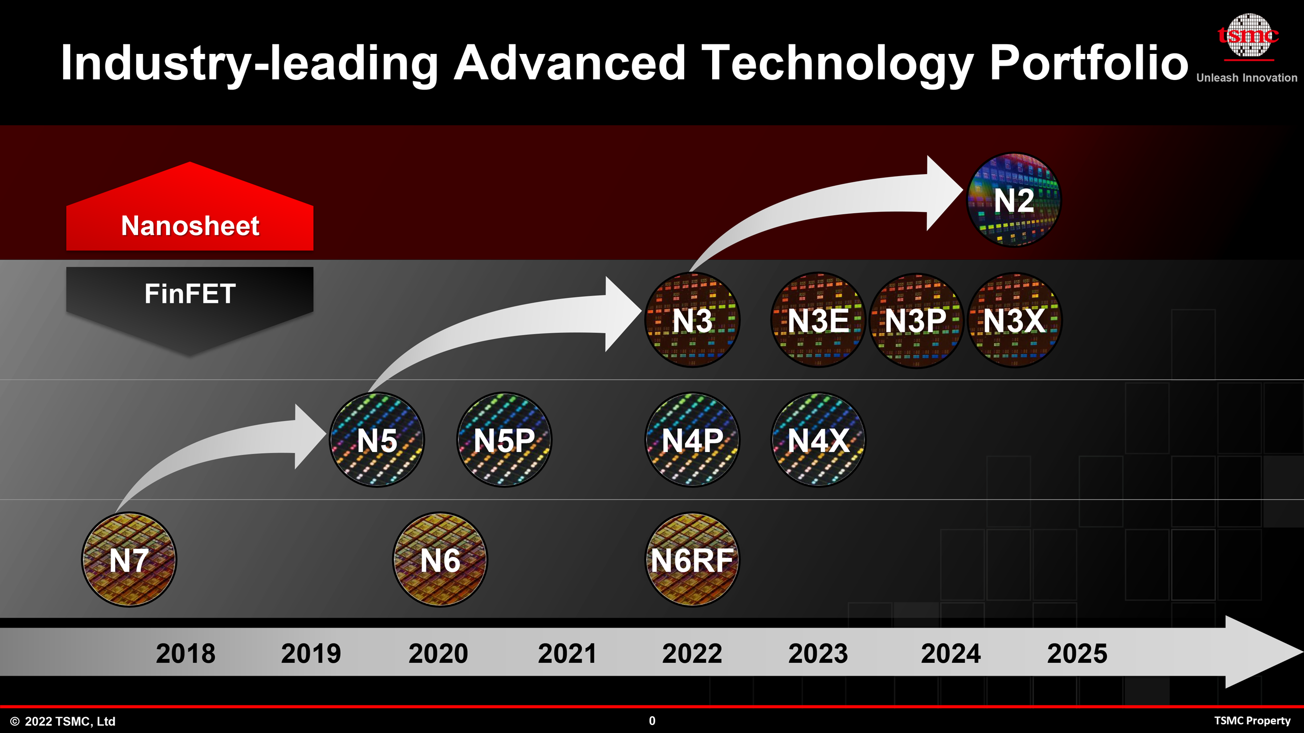
N3: 5 nodes in the next 3 years
As the manufacturing process becomes more complex, so does the time for pathfinding, research and development, so TSMC and other foundries no longer spawn new nodes every two years. With N3, the rhythm of TSMC’s new node introduction extends to about 2.5 years, while with N2 it extends to about 3 years.
In short, TSMC needs to offer an expanded version of the N3 to meet the needs of customers who demand higher performance per watt and higher transistor density each year. Another reason TSMC and its customers need multiple versions of the N3 is that the foundry N2 relies on a brand new gate-all-around field-effect transistor (GAA FET) mounted using nanosheets. is. This is expected to be higher cost and new design. Methodology, new IP, and many other changes. Leading-edge chip developers will soon jump to N2, but many TSMC rank and file customers will stick to a variety of N3 technologies over the next few years.
At the TSMC Technology Symposium 2022, the foundry talked about four N3 derivative manufacturing processes (a total of five 3 nm class nodes) (N3E, N3P, N3S, and N3X) that will be introduced in the coming years. These N3 variants will provide improved process windows, improved performance, increased transistor density, and increased voltage for ultra-high performance applications. All of these technologies support FinFlex, TSMC’s “secret source” feature. This greatly increases design flexibility and allows chip designers to accurately optimize performance, power consumption, and cost.
| Improved PPA advertised for new process technology Data published during conference calls, events, press briefings and press releases |
||||||||
| TSMC | ||||||||
| N4 vs N5 |
N4P vs N5 |
N4P vs N4 |
N4X vs N5 |
N4X vs N4P |
N3 vs N5 |
N3E vs N5 |
||
| Power | low | -twenty two% | ―――― | ?? | ?? | -25-30% | -34% | |
| performance | taller than | + 11% | + 6% | + 15% Also more |
+ 4% that’s all |
+ 10-15% | + 18% | |
| Logic area
Discount *% Logic density * |
0.94x
-6% 1.06x |
0.94x
-6% 1.06x |
―――― |
?? |
?? |
0.58x
-42% 1.7 times |
0.625x
-37.5% 1.6 times |
|
| Volume Manufacturing |
2022 | 2023 | H2 2022 | 2023 | 2023 | H2 2022 | 2nd to 3rd quarter of 2023 | |
* Please note that TSMC only began to publish the analog, logic, and SRAM transistor density extensions separately around 2020. Some numbers reflect a “mixed” density consisting of 50% logic, 30% SRAM, and 20% analog.
N3 and N3E: in orbit of HVM
TSMC’s first 3nm class node is called N3, which is expected to begin mass production (HVM) later this year. The actual chip will be available to customers in early 2023. This technology is primarily targeted at early adopters (such as Apple) who can invest in cutting-edge designs and benefit from performance, power and area (PPA). Benefits provided by state-of-the-art nodes. However, because it is tuned for a particular type of application, the N3 process window is relatively narrow (a range of parameters that produce defined results) and is not suitable for all applications in terms of yield. Not limited.
This is the introduction of N3E. New technologies improve performance, reduce power, and enlarge process windows, resulting in higher yields. However, the trade-off is that the node logic density is slightly reduced. Compared to the N5, the N3E reduces power consumption by 34% (at the same speed and complexity) or improves performance by 18% (at the same power and complexity) and increases the density of logic transistors by 1.6 times.
It is noteworthy that the N3E offers higher clock speeds than the N4X, based on data from TSMC (scheduled for 2023). However, the latter also supports ultra-high drive currents and voltages in excess of 1.2V. At this point, it can provide unmatched performance, but it consumes very much power.
In general, N3E looks like a more versatile node than N3. So it’s not surprising that TSMC has more “3nm tapeouts” at this point than it would have used a 5nm class node at a similar point in development. ..
Risk production of chips using N3E will begin in the coming weeks (ie, Q2 or Q3 2022) and HVM will be set for mid-2023 (again, TSMC will be in Q2 and Q2). We do not disclose which of the three quarters we are talking about). Therefore, commercial N3E chips are expected to be available in late 2023 or early 2024.
N3P, N3S, and N3X: Performance, Density, Voltage
Improvements in N3 are not limited to N3E. TSMC will announce the N3P, a version with improved manufacturing process performance, and the N3S, a flavor with increased density of this node, around 2024. Unfortunately, TSMC currently does not disclose what improvements these variants offer in comparison. To baseline N3. In fact, at this time, TSMC does not show N3S in all versions of the roadmap. So guessing its characteristics is not really a good business.
Finally, for customers who need ultra-high performance regardless of power consumption or cost, TSMC offers N3X, which is essentially the successor to N4X. Again, TSMC hasn’t revealed any details about this node, except that it supports high drive currents and high voltages. It may be speculated that the N4X can use backside power supplies, but I’m not sure if this is the case as FinFET-based nodes and TSMCs only mount backside power rails on GAAFET-based N2s. Nevertheless, TSMC probably has a lot of ace when it comes to rising voltage and improving performance.
FinFlex: N3 secret source
When it comes to extensions, we definitely need to mention FinFlex technology, the secret source of TSMC’s N3. In short, FinFlex allows chip designers to precisely tune building blocks to improve performance, density, and power.
When using FinFET-based nodes, chip designers can choose from different libraries that use different transistors. If the developer needs to minimize die size and save power at the expense of performance, the developer uses a double-gate single fin (2-1) FinFET (see figure). However, if you need to maximize performance with the trade-off between die size and high power, use triple gate dual fin (3-2) transistors. If the developer needs balance, use a dual-gate dual-fin (2-2) FinFET.
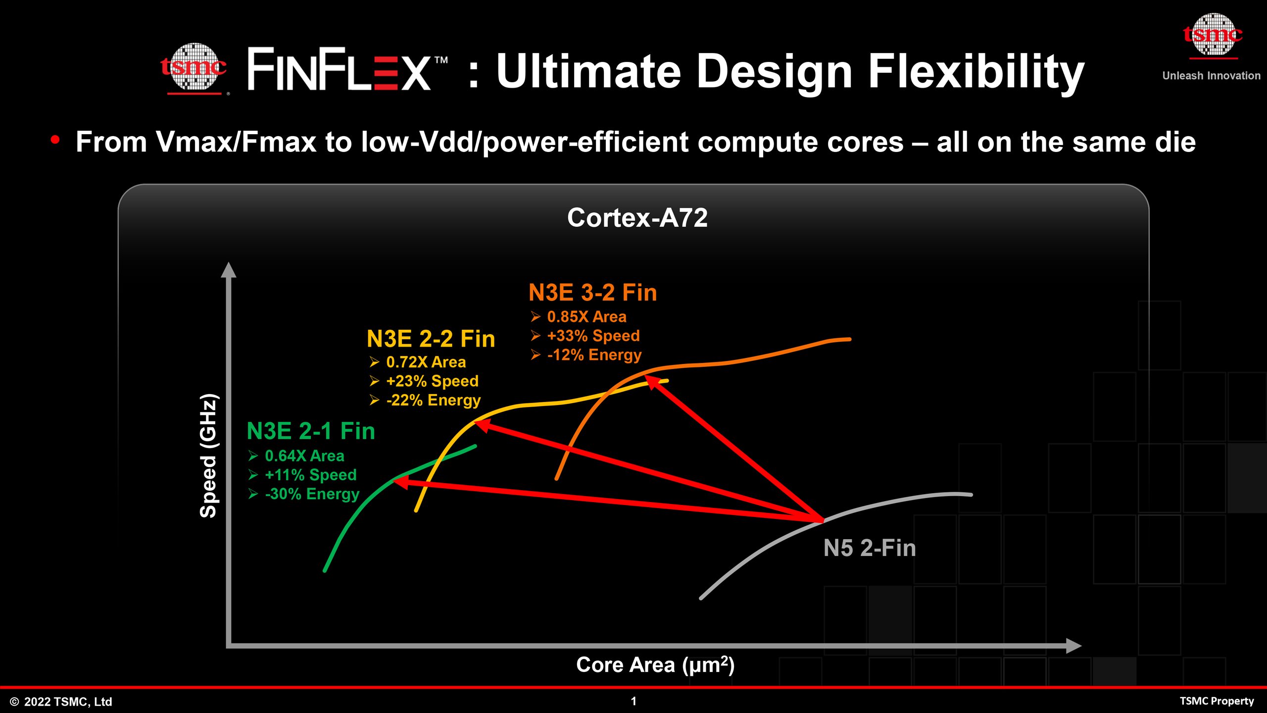
Currently, chip designers need to stick to one library / transistor type for either the entire chip or the entire block of the SoC design. For example, CPU cores can be run faster with 3-2 FinFETs or 2-1 FinFETs can be used to reduce power consumption and footprint. This is a fair trade-off, but not ideal in all cases. Especially if you’re talking about 3nm class nodes, which are more expensive to use than existing technologies.
For the N3, TSMC’s FinFlex technology allows chip designers to combine different types of FinFETs in a single block to precisely adjust performance, power consumption, and area. For complex structures such as CPU cores, such optimization offers many opportunities to improve core performance while optimizing die size. So I’m looking forward to seeing how SoC designers can take advantage of FinFlex in the looming N3 era.
FinFlex is not a replacement for node specialization (performance, density, voltage) because the difference in process technology is greater than the library or transistor structure within a single process technology, but FinFlex is performance, power, and Seems like a great way to optimize costs. TSMC N3 node. Ultimately, this technology brings FinFET flexibility a little closer to GAAFET flexibility. GAAFETs will provide adjustable channel widths for higher performance and lower power consumption.
Overview
Like TSMC’s N7 and N5, the N3 is another family of long-lasting nodes for the world’s largest contrast maker of semiconductors. Especially with the introduction of TSMC’s jump to GAAFETs at 2nm, the 3nm family will be the last family of the company’s “classic” state-of-the-art FinFET nodes, with many customers sticking to it for years (or more). prize. ). That’s why TSMC has multiple versions of N3 tailored to different applications and FinFlex technology that provides chip designers with design flexibility.
The first N3 chips will go into production in the coming months and will hit the market in early 2023. Meanwhile, TSMC will continue to produce semiconductors using N3 nodes ever since it introduced N2 process technology in 2025.


