
The semiconductor industry took more than a decade to prepare everything needed to make chips using extreme ultraviolet (EUV) lithography. It seems that the time it takes to reach the next level, EUV with High-NA, will be significantly reduced.
Need higher resolution
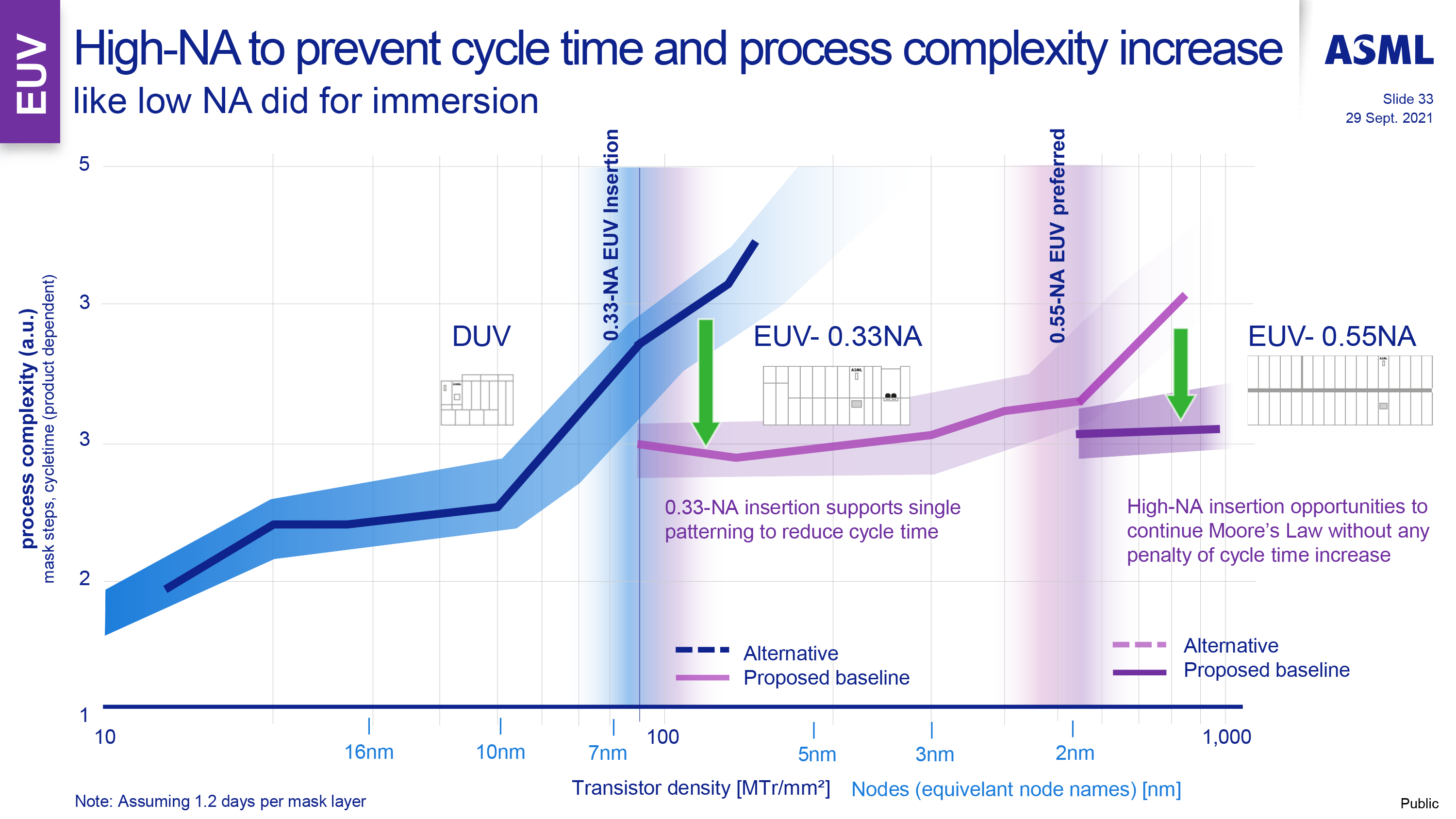
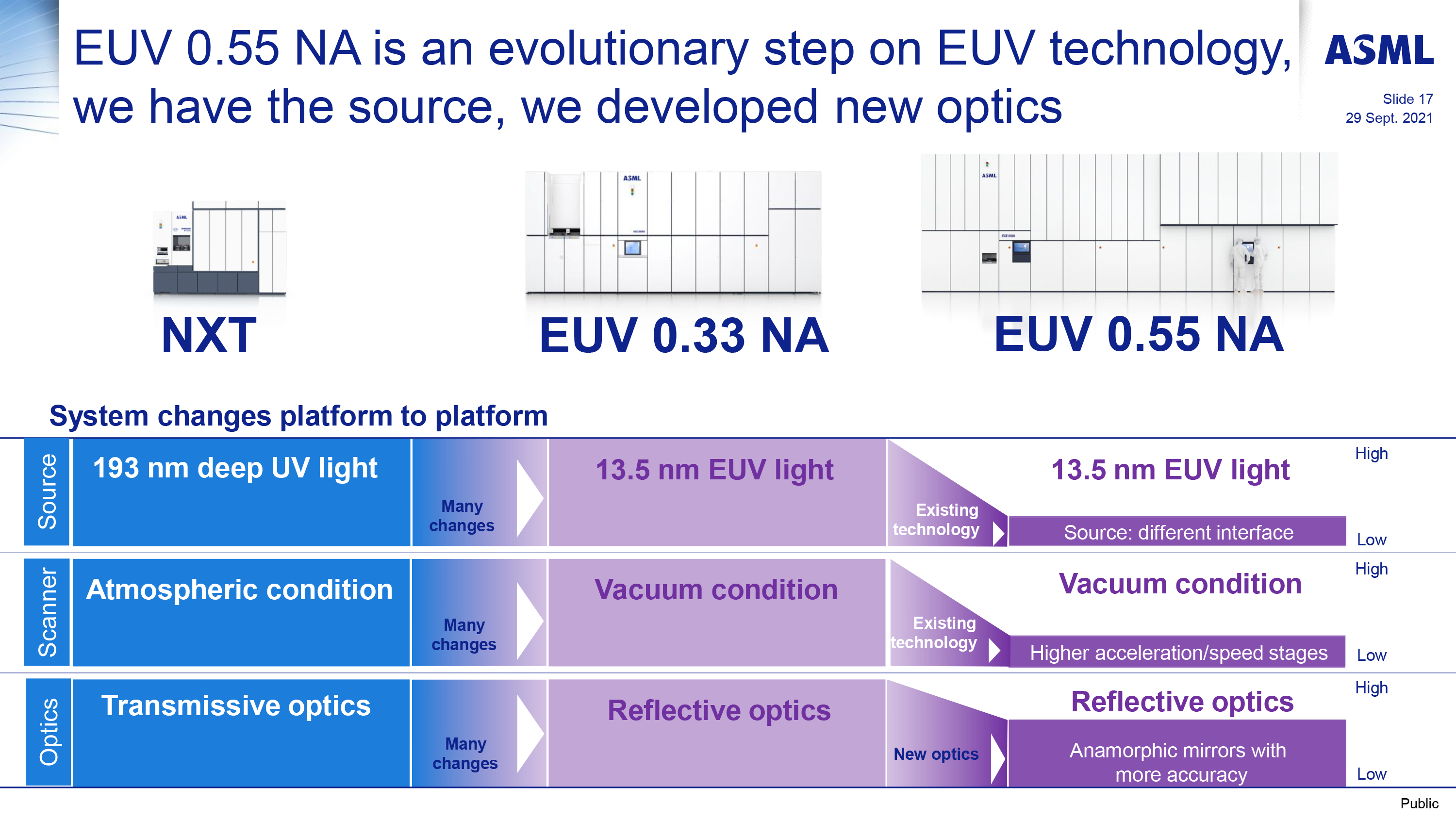
Today, state-of-the-art chips are manufactured in a 5/4 nm class process using the EUV lithography ASML Twinscan NXE: 3400C (and similar) system with a 0.33 numerical aperture (0.33 aperture) that provides 13 nm resolution. NA) Equipped with an optical system. This resolution is sufficient for a single pattern approach at 7nm / 6nm nodes with a pitch of 36nm to 38nm and 5nm with a pitch of 30nm to 32nm. However, if the pitch is below 30 nm (above the 5 nm node), a resolution of 13 nm may require dual lithography exposures that will be used for years to come.
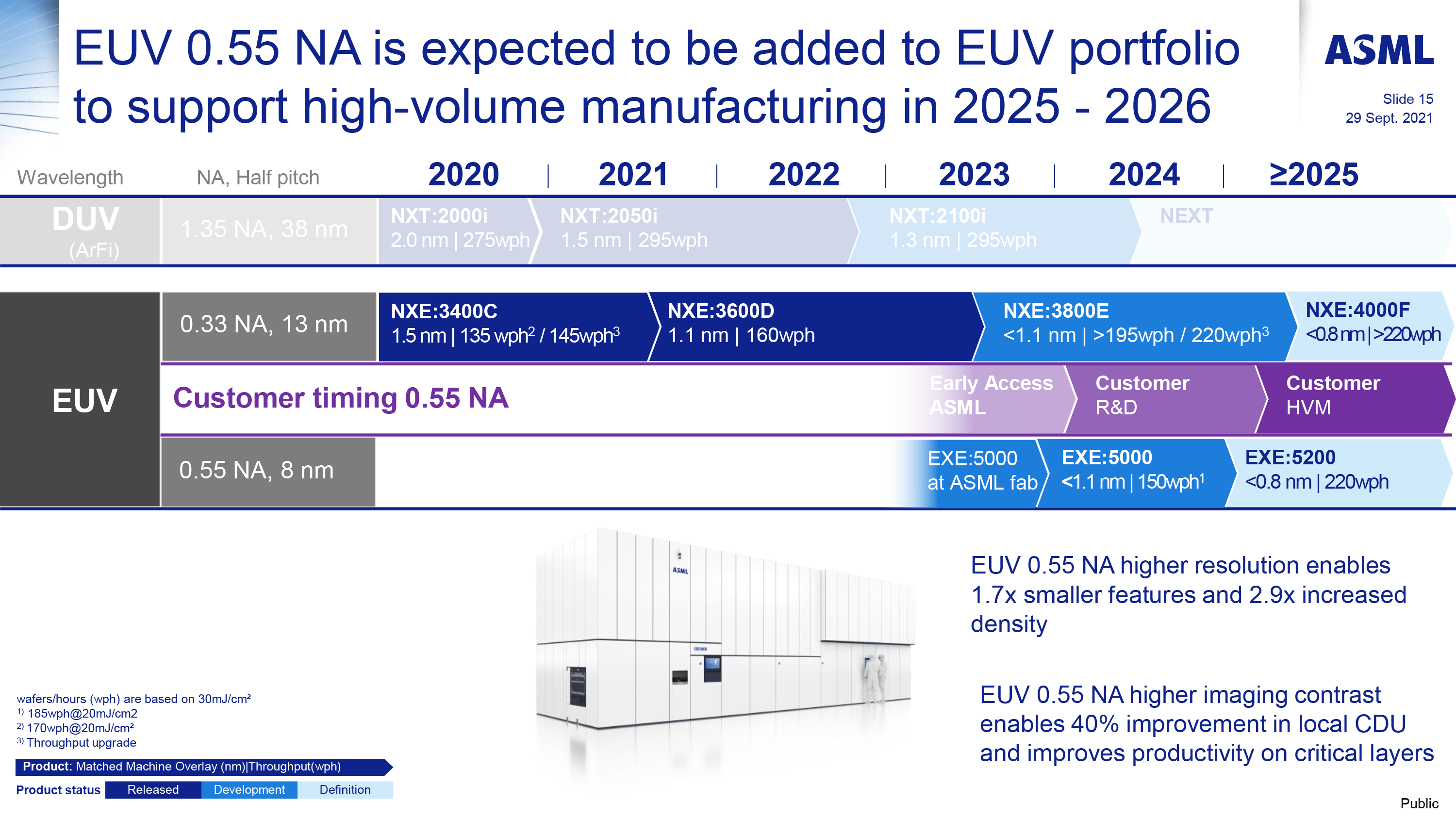
For the post 3nm node, ASML and its partners are Twinscan EXE: 5000, a new EUV tool with a 0.55 NA (High-NA) lens capable of 8nm resolution, projected to avoid multi-patterning. I’m working on a series. At 3 nm and above. The new High-NA scanner is still under development and is expected to be very complex, very large and expensive. Each costs over $ 400 million. High-NA requires not only new optics, but also new light sources. In addition, we will need new fab buildings to accommodate larger machines. This requires a large investment.
However, leading manufacturers of logic chips and memory devices are aggressively adopting new technologies to maintain semiconductor scaling performance, power, area, and cost (PPAc), and High-NAE UV scanners are for post 3nm. It’s very important. node. As a result, the demand for High-NA tools is quite high.
10-20 High-NA systems provided
A few weeks ago, ASML Disclosure In the first quarter of 2022, we received multiple orders for the High-NA Twinscan EXE: 5200 System (EUV 0.55 NA) from both Logic and DRAM customers. Last week, it revealed that there were 5 orders for the Pilot High-NA Scanner scheduled to be delivered in 2024, and “more than 5” orders for the highly productive follow-on model to be delivered after 2025. did. Reuters..
Interestingly, from 2020 to 2021, ASML said it received High-NA commitments from three customers on a total of up to 12 systems. Logic makers have promised Intel, Samsung Foundry, and TSMC to acquire a prototype High-NA scanner from 2020 to 2021, usually with state-of-the-art tools first in mind. There is no doubt. In addition, ASML has already begun building the first High-NA system, which was completed in 2023. Imec and ASML customerss R & D purpose..
“For High-NA EUV, we are on track and are now beginning to integrate the first High-NA system into our new clean room in Feldhofen.” Said Peter Wennink, Chief Executive Officer of ASML. “We received multiple orders for the EXE: 5200 system in the first quarter. We also received orders for additional EXE: 5200 in April this month. These reservations resulted in three Logic and two Memory customers. We have an order for High-NA from. EXE: The next model of 5200 ASML, the High-NA system, provides the next step in lithography performance and productivity. “
ASML’s Twinscan EXE: 5200 is considerably more complex than a regular Twinscan NXE: 3400C machine, so building these tools will take longer. The company hopes to be able to offer as many as 20 High-NA systems in the medium term. This probably means that customers have to compete for these machines.
“We are also in talks with our supply chain partners to secure capacity for about 20 EUV 0.55NA systems in the medium term,” Wennink said.
Intel first adopts prototype tool
So far, the only process technology that has been confirmed to use ASML’s High-NA tools is Intel’s 18A node, which will be in large quantities in 2025 when ASML begins offering High-NA EUV systems for production. It was planned to start production. But recently, Intel pulled production of the 18A into the second half of 2024, showing that ASML’s Twinscan NXE: 3600D or NXE: 3800E could be used to manufacture the 18A, perhaps through multi-patterning.
Intel’s 18A technology benefits a lot from the High-NAE UV tool, but Intel doesn’t seem to necessarily need a Twinscan EXE: 5200 machine for this node. The use of multi-patterning on commercial chips can increase product cycles, reduce productivity, increase risk, and reduce yield (although the latter is not cast into stone). Still, Intel seems to want the 18A node to arrive as soon as possible. Probably because we consider it to be the primary tool that can regain process technology leadership from TSMC. As a result, Intel’s updated plan will phase out High-NA tools during the 18A lifecycle if the tools are completed on time.
Of course, it is unclear whether using a 0.33 NA EUV scanner for the 18A will provide sufficient productivity for Intel and Intel Foundry Services customers. But at least in 2024, Intel has no choice but to use the machine it owns.
Other major semiconductor manufacturers such as TSMC, Samsung, SK Hynix and Micron will also inevitably adopt High-NAEUV for mass production of chips. The only question is when this is set exactly when this happens.


