
In addition to updating the Zen CPU architecture and RDNA client GPU architecture, AMD is also updating the roadmap for Instinct products related to the CDM server GPU architecture this afternoon. And while CPUs and client GPUs are undoubtedly on a fairly simple path over the next two years, AMD plans to make a major overhaul of its server GPU products.
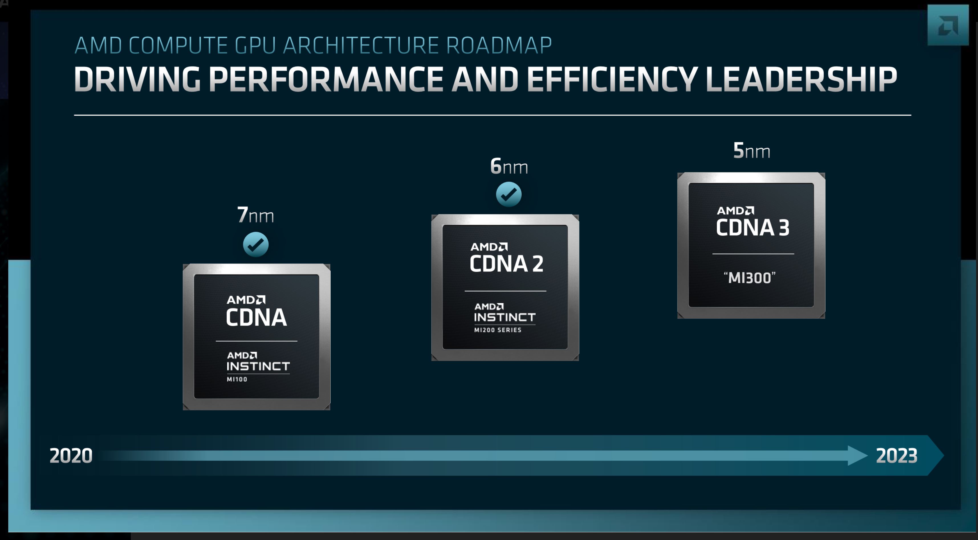
Let’s start with AMD’s server GPU architecture roadmap. Following AMD’s current cDNA 2 architecture used in the MI200 Series Instinct Accelerators, it will be cDNA 3. Unlike other AMD roadmaps, the company does not offer a two-year view here. Instead, the server GPU roadmap is one year (until 2023), and AMD’s next server GPU architecture will be available next year.
The first time I saw CDNA 3, it was quite detailed. With its launch in 2023, AMD isn’t as restrained as anywhere else. As a result, everything is exposed, from the architecture to the basic information about the data center APU, which consists of a CPU and GPU chiplet, one of the products that incorporates cDNA 3.
From the top, GPUs based on the CDM 3 architecture are built on the 5nm process. It also relies on chiplets to combine memory, cache, and processor cores all into one package, similar to previous cDNA 2-based MI200 accelerators. In particular, AMD calls this a “3D chiplet” design. This means that not only chiplets are stacked on the board, but some chips are stacked on top of other chiplets, AMD’s V-. Cache for Zen3 CPU.
This comparison is particularly relevant here as AMD plans to introduce Infinity Cache technology to the CD DNA3 architecture. Also, judging from AMD’s artwork, as in the V-Cache example above, it looks like the logic is stacked in the cache as a separate die rather than being integrated into a monolithic die like a client GPU.Due to this stacked nature, the Infinity Cache chiplet for CDN A3 under Processor chiplet. AMD seems to have a very power-intensive logic chiplet at the top of the stack for effective cooling.
CDNA 3 also adopts AMD 4th Generation Infinity Architecture. We’ll talk more about this in another article, but in a short version, for GPUs, IA4 is closely tied to AMD’s chiplet innovation. Specifically, it makes 2.5D / 3D stack chips available to the IA, allowing all chips in the package to share an integrated, fully coherent memory subsystem. This is a huge leap beyond the IA3 and current MI200 accelerators. These accelerators provide memory consistency, but do not have a unified memory address space. Therefore, the MI200 accelerator basically functions as two GPUs in one package, but in IA4, despite the decomposed nature of the chiplet, the cDNA 3 / MI300 accelerator operates as a single chip. I can.
AMD’s figure also shows that HBM memory is being used again here. AMD hasn’t specified a version of HBM, but given the time frame of 2023, it’s very safe to be HBM3.
Architecturally, AMD will take several steps to improve the AI performance of high performance accelerators. According to the company, they are adding support for new mixed-precision math formats. Although not explicitly stated today, more than a five-fold improvement in performance per watt for AMD’s AI workloads strongly suggests that AMD is significantly reshaping and extending the CNDA 3 matrix core. I am. Five times more than is possible with fab improvements alone. delivery.
MI300: AMD’s first non-aggregated data center APU
However, AMD not only builds larger GPUs, but also integrates memory pools with a multi-chiplet architecture to run GPUs in shared memory pools. Instead, AMD’s ambitions are much greater than that. With the freedom to use high-performance CPU and GPU cores, AMD has taken the next step in integration to build a non-intensive data center APU that is a chip that combines CPU and GPU cores into a single package. I am.

The data center APU, now codenamed MI300, has been built by AMD for some time. MI200 and Infinity Architecture 3 allow AMD CPUs and GPUs to work with coherent memory architectures, and for some time the next step was to further integrate CPUs and GPUs in terms of both packaging and memory architecture.
Especially when it comes to memory issues, the integrated architecture brings some great advantages to the MI300. From a performance standpoint, this remedies the problem by eliminating redundant memory copies. Processors no longer need to copy data to a dedicated memory pool to access / modify that data. The integrated memory pool also means that you don’t need a second pool of memory chips. In this case, it is usually the DRAM connected to the CPU.
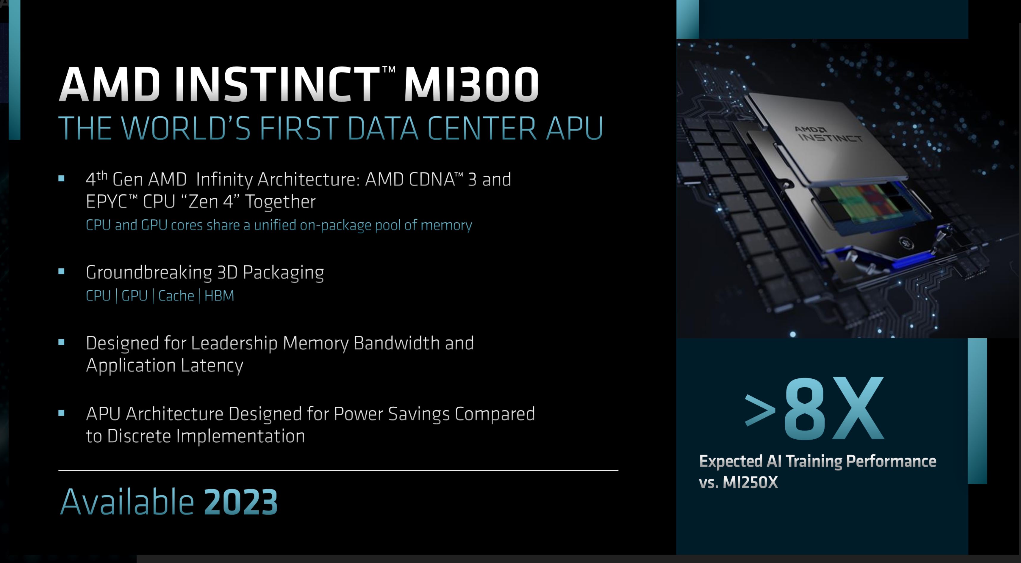
The MI300 integrates a CDEN3 GPU chiplet and a Zen4 CPU chiplet into one processor package. Both of these processor pools share HBM memory on the package. And perhaps Infinity Cache as well.
As mentioned earlier, AMD will make extensive use of chiplets to achieve this. CPU cores, GPU cores, Infinity Cache, and HBM are all different chiplets, some of which are stacked on top of each other. So this is a chip, unlike what AMD has built so far, and integrating chiplets into product design will be AMD’s most complex effort to date.
AMD, on the other hand, is very clear about the fact that it is aiming for market leadership in terms of memory bandwidth and application latency. If AMD can make it successful, it will be an important achievement for the company. That said, it’s not the first company to pair HBM with CPU cores. Intel’s Sapphire Rapids Xeon CPU claims its achievements. So it’s interesting to see how the MI300 works in that regard.
For more specific issues with AI performance, AMD claims that APU offers training performance that is eight times better than the MI250X accelerator. This further demonstrates that AMD makes some major enhancements to the GPU Matrix core compared to the MI200 series.
Overall, AMD’s server GPU trajectory is pretty similar to what Intel and NVIDIA announced in the last few months. All three companies are building for CPU and GPU combination products. NVIDIA with Grace Hopper (Grace + H100), Intel with Falcon Shores XPU (CPU + GPU combination), and MI300 with both CPU and GPU chiplets in one package. In all three cases, these technologies aim to combine the best CPUs and the best GPUs for workloads that aren’t completely constrained to either. For AMD, the company believes it has the best CPU and the best GPU built into it. To process.
We expect to see more about CD DNA3 and MI300 in the coming months.


