
TSMC officially opened its Advanced Backend Fab 6 facility on Friday. The facility will be used to expand the company’s ability to build high-end multi-chiplet products. The facility is said to be the first all-in-one automation fab to offer 3DFabric integration of front-end to back-end processes and test services.
TSMC’s advanced back-end Fab 6 is capable of processing approximately 1 million 300mm wafers per year and over 10 million hours of testing per year. The plant occupies 14.3 hectares within the Chunan Science Park and has more cleanroom space than all of TSMC’s other advanced back-end factories combined, making it TSMC’s most advanced to date, according to the company. It is said that it has become a typical packaging facility.
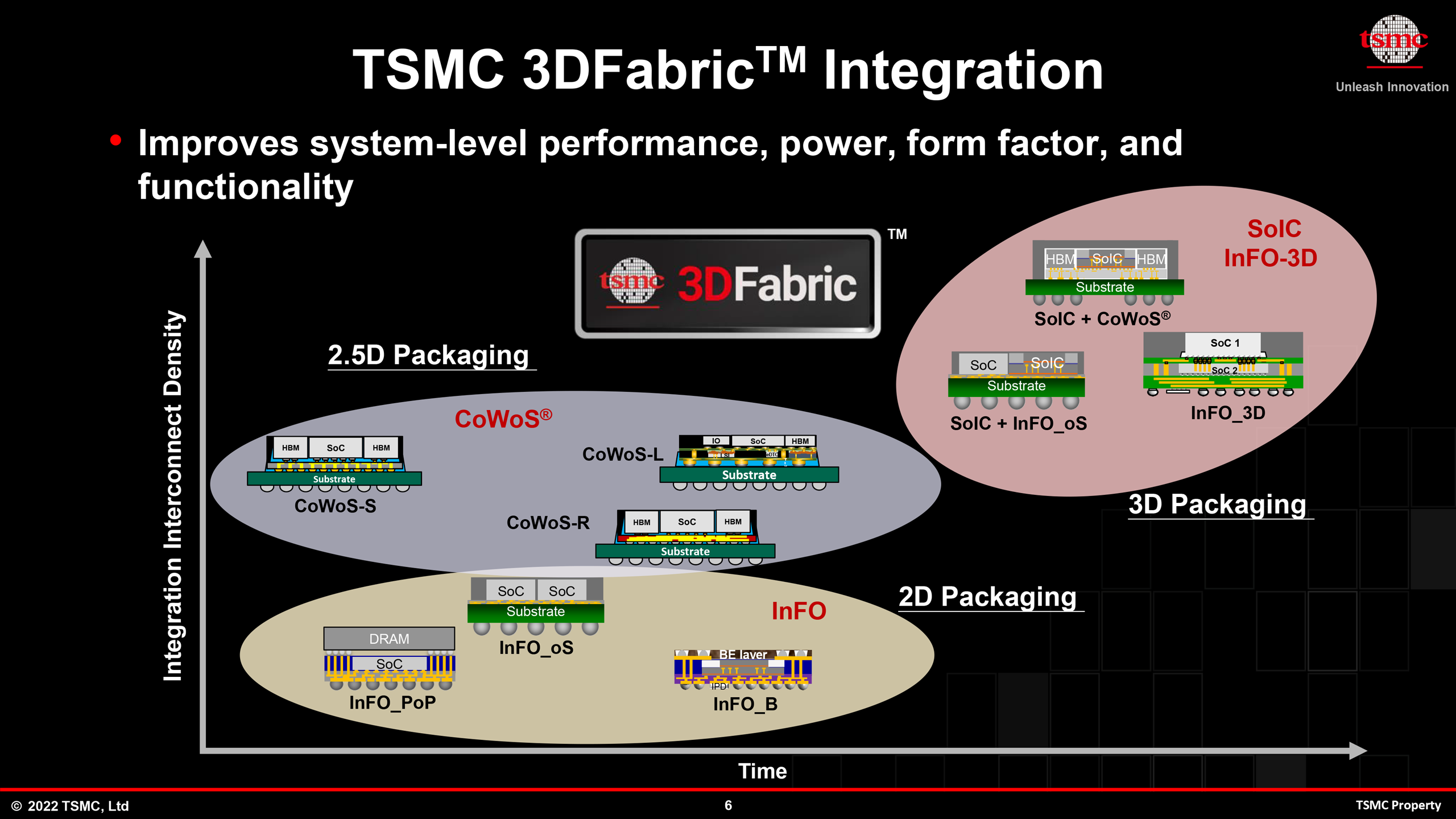
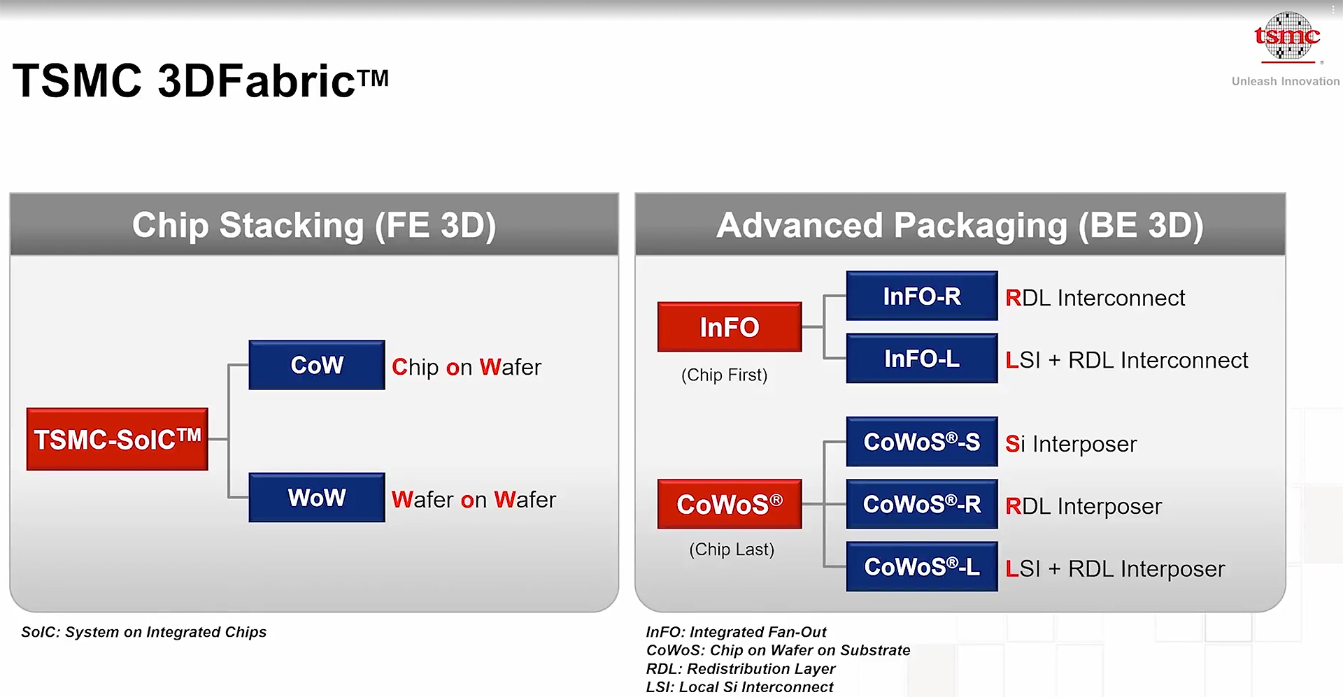
TSMC says Advanced Backend Fab 6 will be ready for volume production of TSMC-SoIC (System on Integrated Chip) process technology, including front-end 3D stacking technologies such as Chip-on-Wafer (CoW) and Wafer-on-Wafer (WoW). said it is done. ). The fab is also behind advanced back-end packaging technologies such as Integrated Fan-Out (InFO) and Chip-on-Wafer-on-Substrate (CoWoS) used in chips like Apple’s M2 Ultra, AMD’s Instinct MI300 and NVIDIA. Designed to handle. A100 and H100.
“Chiplet stacking is a key technology for improving chip performance and cost-effectiveness.In response to strong market demand for 3D ICs, TSMC will be the early adopter of advanced packaging and silicon stacking technology production capacity. and provide technology leadership through the 3DFabric platform,” said Dr. Jun He, Vice President of Operations/Advanced Packaging Technologies and Services, and Quality and Reliability.
Perhaps the most notable feature of TSMC’s Advanced Backend Fab 6 is its comprehensive 5-in-1 intelligent automated material handling system with a total length of over 32 kilometers. Production information from wafer stage to die is integrated with the dispatching system to speed up the manufacturing cycle. The process is AI-enhanced for precise process control and real-time defect detection to maximize yield. Because when packaging a multi-chiplet solution like AMD’s MI300, any anomaly at the package level immediately disables all chiplets above it, costing you thousands of dollars at least. , which is especially important. This factory processes 500 times more data per second than a typical front-end factory, enabling a complete manufacturing history for each die, allowing foundries to track each die processed through the factory. will be
“With production capacity to meet customer needs, together we will unleash innovation and become an important partner that customers can rely on for the long term,” added Jun He.


