
TSMC announced Tuesday plans to build a new advanced chip packaging facility at Causeway Science Park. The company plans to spend about $2.87 billion on the plant, which will employ about 1,500 people when it goes live in the next few years.
“To meet the needs of the market, TSMC plans to establish an advanced packaging factory at Tongluo Science Park,” a TSMC statement said. “TSMC expects to invest nearly NT$90 billion in this project and create employment opportunities for 1,500 people. The Science Park Administration has formally agreed to TSMC’s application for land lease in Causeway Science Park and is arranging a lease presentation.”
It will be years before the chip-packing site itself goes online. TSMC hasn’t even started ground preparations yet, and the company hasn’t announced an official date for the project’s completion, but local media in Taiwan are reporting that the factory will be up and running sometime in 2027.
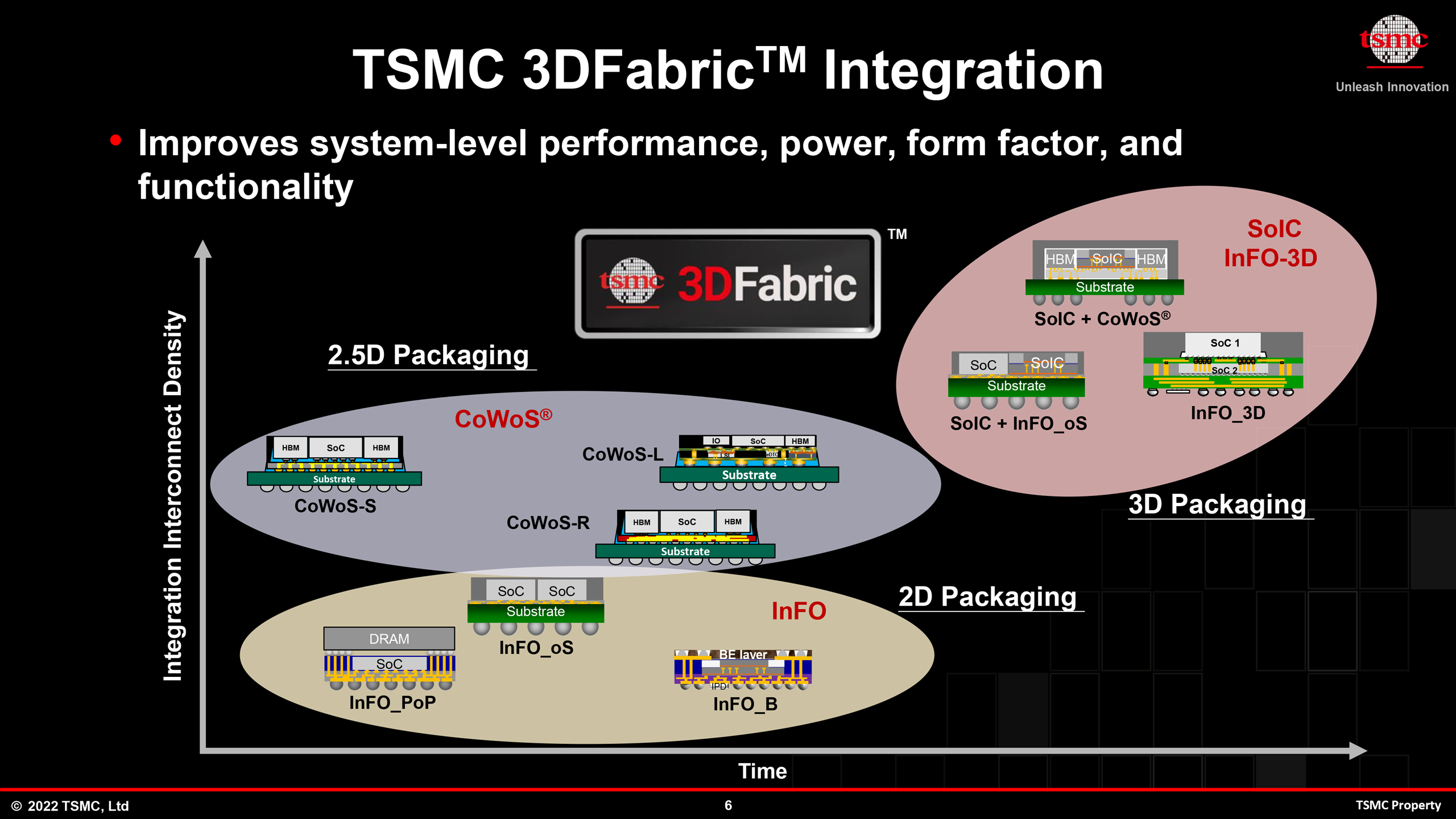
Otherwise, a price tag of around $2.9 billion means this will be an even more significant capital expansion project for TSMC, rivaling the cost of a wafer lithography fab a decade ago. Considering TSMC’s product roadmap and the forecast that the need for advanced packaging types will increase in the next few years, the new chip packaging fab is likely to be a comprehensive facility providing 3DFabric integration and testing services for front-end to back-end processes.
The new Tongluo Fab will be Akin TSMC’s recently opened Advanced Backend Fab 6, which is designed to support the TSMC-SOIC (System on a Chip) process technology.
TSMC’s InFO and CoWoS packaging technology is currently used in chips such as Apple’s M2 Ultra, AMD’s Instinct MI300 and NVIDIA’s A100 and H100 GPUs. Demand for the latter has skyrocketed recently, and TSMC admitted just last week that it doesn’t have enough CoWoS capacity to keep up. As it stands, the company is working hard to double his CoWoS capacity by the end of 2024.
“But when it comes to the back-end, the advanced packaging side, especially CoWoS, our capabilities are very limited and it is very difficult to meet 100% of what our customers need,” TSMC Chief Executive CC Wei said at an earnings call last week. “So we are working together in the short term to meet customer demand, but we are increasing capacity as soon as possible. […] I can’t tell you the exact numbers [in terms of processed wafers capacity]but CoWoS [capacity will be doubled in 2024 vs. 2023].
TSMC’s advanced back-end Fab 6 can process approximately one million 300mm wafers per year, as well as more than 10 million hours of testing per year. It’s unclear what capacity the upcoming packaging plant will have, but with the growing importance of advanced packaging, it’s reasonable to expect TSMC to expand the plant even further.


